
Oscilloscope Clock II - An Essay*
Introduction
The origin of this clock lies with the superb designs by David Forbes that can be found here, here and here. I cannot place sufficient emphasis on the fact that without this inspiration and the schematics placed in the public domain by David (as licenced), that my own clock would never, ever have got off the ground.
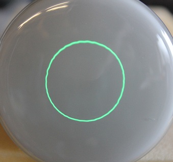
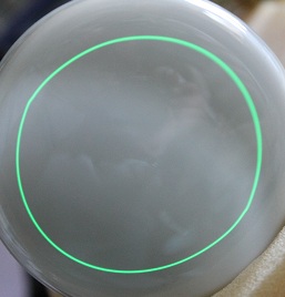
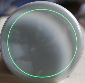
What makes this type of clock special is how the image is created. Many other scope clocks (including my own scope clock 1) use a pair of DACs to drive the CRT deflection amplifiers directly. Objects (lines, circles, arcs) are created by varying the DAC output in steps to move the beam about. Such displays can be "pixelated" in appearance - straight lines can appear with "jaggies". The design by David Forbes uses sine and cosine signals applied to the deflection amplifiers to generate a completely smooth and round circle (lines, arcs, ovals are generated in a similar manner). Such a display technique creates objects with no digital effects, pixelation, jaggies etc.
At least one other person has modified and produce this type of circle scope clock and details can be found here. Well done!
This page does not describe a scope clock fully built, cased and finished. But it does describe a fully working design that could easily be progressed to completion. This is a snapshot of my fully working test bed for ideas, alternatives and experiments; as I said it is an essay* in the craft.
N.B. I do not assemble kits for this clock!Quick Links
- introduction
- a quick look
- photo gallery
- download stuff here
- schematics and PCBs
- software
- where am I going next?
- parts list
- how it works
- further information A: developments and other CRTs
- further information B: low cost PSU & trace rotation
Preview

It's a mess, but it's a working mess….
Gallery
Hover the mouse for more information.
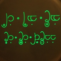
Titles

Some analogue faces


Binary and BCD


Digital


Other clocks


Astronomical


Four letter words
")
Play time

Behind the scenes
Fonts


")
")

System data

Menu illustrations

 Quick Links
Downloads
You should look in the "/CRT Projects/Scope Clock 2 - Volume I" folder.
Quick LinksSchematics and Layouts
The schematics and PCB layouts were created using Eagle and are available for download here.
As always I am willing to make the PCBs (at cost) for anyone wanting to attempt this clock.
(This clock has been built and tested using only a DG7/32 CRT but it intended that it can be adapted to other CRTs.)
Unfortunately I have lost my ability to make PCBs at home and so I cannot offer PCBs for this clock anymore.
The component parts lists are available in the Annexes.
A detailed explaination of how the clock works (with simplified schematics) is available in the Annexes.
Power supply
I used a couple of mains transformers to make a huge brick of a power supply - but it is simple, robust and should be easy to adapt to the requirements of other CRTs.
Transformer board

For ridgity and tidiness I mounted the two transformers on an otherwise almost bare PCB with rows of header pins to take the transformer wiring and the wiring to the PSU PCB proper. A mains fuse and mains screw connector completes the board.


Main Power Supply
This board carries a number of rectifiers and electrolytic capacitors to get the range of voltages required by the CRT. So that the high negative voltages used on the cathode, control grid and focus anode (or grid) did not have to connect to other boards I put the focus and brightness controls, and the blanking amplifier on this board as well.

The board was designed so that it could be stacked on the transformer board and the incoming wiring positions match the wiring on the transformer board so only simple straight links are required. (N.B. One of the three trim pots visible has been replaced by a fixed resistor in the final design.)


Analogue card

This board carries two identical amplifiers to drive the deflection plates of the CRT. The positive high voltage from the PSU card is stabilised at 240V (with respect to ground, about 650V with respect to the cathode) using two zener diodes. A centre tap on these zener diodes is used to supply the final anode.
The board also carries the analogue parts of the sine and cosine generators, the shape selector and DACs.
The analogue components have their own regulators providing ±5V and ±12V.
Connections to the main PSU and the CRT are made using wires on header pins, and connection to the digital card using a 10way ribbon cable.


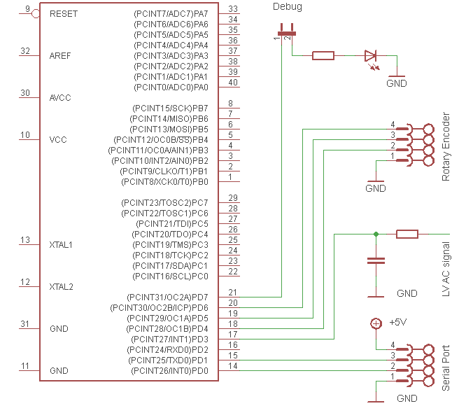
Digital card

The digital carries two Atmel AVR microcontrollers. An atmega1284p modestly overclocked at 22.1184MHz is the main controller. The second AVR is a attiny26 (clocked at 16 MHz) and is dedicated to sine and cosine generation (as squarewaves), CRT blanking logic and image synchronisation. The card also has the RTC (with its battery), chimes generator and its own 5V stabilised PSU. Connections are mostly made using wires on pin headers but the connection to the analogue card is made using IDC connectors and a 10 way ribbon cable.

 Quick Links
Software
I have written most of this software and it is released under the terms of the GNU General Public License Version 2 (each file should contain a full statement). However, I wish to acknowledge that the file font.c contains (a tweaked version of) the font created by David Forbes and the file has his copyright notice as well.
The software was written in ASM and C for the AVR-GCC compiler. The full source code and makefiles are available for download here.. This zip files contains the current version and was used. I include it here for anyone to download and to read through to see how aspects of the code work. But I do not intend this to be the final version and suggest anyone attempting to build this clock should contact me for the current version.
The mine directory contains my common libraries that the scope clock uses. These should be placed in a directory and the makefile edited so the compiler can find them. The cfg directory contains hardware configuration .h files and should exist as a subdirectory of the main project directory (or edit the makefile).
The code for the atmega is written in several layers:
| CRT Driver & Timing crt.* crtasm.S |
|||||
| Hardware Servicing services.* |
Chime Generation chime.* |
Clock Configuration config.* |
|||
| Object Creation and Drawing draw.* font.* |
|||||
| Menus menu.* menu_rtc.* menu_latlong.* |
|||||
| Clocks analogue.* bcdclk.* binary.* digital.* droplet.* elvish.* flip.* klingon.* pinpong.* sidereal.* |
Displays bounce.* flw.* sunarc.* title.* |
||||
- The lowest layer (top in the table) is the fast CRT driver in crt.h, crt.c and crtasm.S; written in C and ASM and it takes object data from a data buffer and draws it to the CRT. The .S file also contains the mains frequency interrupt that is used to initiate a screen refresh (also written in ASM) and carries out various other timing functions.
-
- Files services (.c .h) contains a number of miscellaneous functions that main of the clocks require to operate and that cannot be placed more logically in another file.
- Files chimes (.c .h) contain the low level driver for the chimes hardware. The timing of the chiming uses the mains interrupt code.
- Files config (.c .h) hold the user changeable settings (which are protected by a checksum). As a rule, user settings that might change frequently are saved to the RTC NVR. User settings that might change infrequently, or that the user may never feel the need to change are saved to the atmega's EEPROM.
-
- Files draw (.c .h) contain contain drivers to create primative objects and so has functions like drawLine(…) and drawCircle(…). Attributes such as object brightness, text scaling and justification, text underlining, text kerning and object blinking are controlled. Also defined is a function that will take a list of primative ojects to form a compound object called a "shape".
- Also at this level are files font (.c .h) that contains the definitions of all the character and symbols that can be drawn.
-
- Files menu (.c .h) operate the menu system. Any displayed clock or other display can be "clicked" by pressing the button on the encoder. A menu system is entered where display parameters, the date and time and so on can be changed. The menu system allows numerical values to be changed and values selected from radiobuttons and logical states toggled using checkboxes.
- Files menu_rtc (.c .h) allow the registers of the RTC to be changed or inspected and files menu_latlong (.c .h) allow the user's latitude and longitude to be entered which are needed by the astronomical calculations.
- At the highest level, files (.c .h) analogue, bcdclk, binary, bounce, digital, droplet, elvish, flw, klingon, pingpong, sunarc and title all contain the code for a particular clock face or other such final display.
The code for the attiny is in the sine directory and written entirely in ASM. It has its own makefile which you will find in the directory as well.
Quick LinksNext steps
So where am I going next with this clock? I need to polish some aspects of the software and carry out some further testing; I also have several other clock faces to add as well as further astronomical displays (sidereal time and moon rise/set/phases).
I want to test other CRTs, including the DH3/91 I used in scope clock 1 and try beam modulation by PWM for brightness control.
Build and case a complete clock, probably using a DG7/32 unless something else comes along. Seek permission from SHMBO to bring it into the house (tough one).
I also need to work on a flyback convertor based PSU to reduce the size of the power supply brick to that of a small pebble. And build and test EHT multipliers so tubes with a PDA can be used (I have a DG10/18 CRT waiting for this.)
Quick LinksAnnexes
Parts Lists
None of these components should be difficult to source. At the time of writing this webpage the tube and its socket are readily available from tube suppliers and Ebay. A number of the components (especially the electrolytic capacitors) are size critical, so be sure to buy the correct diameter components if the parts are not sourced from Farnell or Rapid; or modify the board of course.
These parts lists are "work in progress" and, as such, are incomplete. It's a dull job to update them and I'm having too much fun with the clock software… and now future projects.
Transformer Board Parts List
| Part | Description | Farnell Code | Rapid Code | Dimensions |
| Transformer A | 230V 10mA, 13.5V 200mA, 6.3V 1A | Transformer TRA800 from Ask Jan First |
||
| Transformer B | 2 x 22V 1.6VA | 9531360 | ||
| F1 | 0.5A | 26-0167 | 20 x 5mm holder | |
| X1 | Transformer B wires | see note 1 | ||
| X2 | Mains supply | screw connector, 5.08mm spacing, 3 way | ||
| X3 | Outputs to PSU PCB | see note 1 | ||
| X4 | Transformer A wires | see note 1 | ||
Notes
- 0.1" pin header strip with everyother pin removed; wires soldered and covered with heatshrink tube
Power Supply Board Parts List
| Part | Description | Farnell Code | Rapid Code | Dimensions |
| C1 | 100u 16V | 1236662 | ||
| C2 | 2200u 16V | 9692215 | This part is 25V | |
| C3 | 10u 16V | 9451480 | ||
| C4, C5 & C6 | 100n | 9750983 | ||
| C7, C8 & C11 | 220u 400V | 8813582 | ||
| C9, C12, C14 & C15 | 100u 250V | 1673472 | ||
| C10 | 1u 630V | 1200810 | ||
| C13 | 1u 250V | 9693980 | ||
| R1 | 390 5% 0.25W | 62-0360 | ||
| R2 | 1k trim pot | 9354298 | Bourns 3362P series; see note 2 | |
| R3 | 330 5% 0.25W | 62-0358 | ||
| R4 | 10k 5% 0.25W | 62-0394 | ||
| R5, R7, R8, R12, R13 & R16 | 470k 5% 0.25W | 62-0434 | ||
| R6 | 1M8 5% 0.25W | 62-0448 | ||
| R9, R11, R14 & R15 | 180k 5% 0.25W | 62-0424 | may need adjustment on test | |
| R10 | 500k pot | 9354395 | focus control; see note 3 | |
| D1 & D2 | 1N4001 | 9564993 | ||
| D3 | UF1G | 1625267 | ||
| D4 | 1N4148 | 9565124 | ||
| D5, D7 & D9 | 1N4007 | 9565051 | ||
| D6, D8 & D10 | 150V 1W zener | 9558373 | These ar 5W parts but they fit the board | |
| D11 & D12 | 1N4004 | 1843708 | ||
| Q1 | BC327 | 9558489 | ||
| Q2 | ZTX558 | 9526676 | ||
| IC1 | 78L05 | 1014073 | The pcb layout shows TO220 package; the L device is adequate | |
| IC2 | 6N137 | 9994866 | ||
| X1 | Connection to CRT heater | see note 1 | ||
| X2 | Blanking input from digital card | see note 1 | ||
| X3 | External brightness control (if used) | see notes 1 & 2 | ||
| X4 | Connection to CRT cathode, control grid and focus anode | see note 1 | ||
| X5 | Connection to analogue card | see note 1 | ||
| X6 | External focus control (if used) | see notes 1 & 3 | ||
| X7 | Connection to transformers | wire links or else see note 1 | ||
| X8 | Connection to digital card | see note 1 | ||
| socket for IC2 | 8 pin DIL socket | 22-0107 | ||
Notes
- 0.1" pin header strip with everyother pin removed; wires soldered and covered with heatshrink tube
- The brightness control (R2) can be either a 1k trimpot on the PCB or an external mounted 1k pot connected using X3
- The focus control (R10) can be either a 500k trimpot on the PCB or an external mounted 500k (or 470k) pot connected using X6
Digital Card
| Part | Description | Farnell Code | Rapid Code | Dimensions/Comments |
| R1, R2, R9, R12, R13 | 10k 5% 0.25W | 62-0394 | ||
| R3, R4 | 3k3 5% 0.25W | 62-0382 | ||
| R5 | 1k5 5% 0.25W | 62-0374 | ||
| R6 | 100R trimpot | 9354280 | Bourns 3362P series | |
| R7 | 2k7 5% 0.25W | 62-0380 | ||
| R8 | 15k 5% 0.25W | 62-0398 | ||
| R10 | 5k trimpot | 9354379 | Bourns 3362P series | |
| R11 | 50k trimpot | 9354387 | Bourns 3362P series | |
| C1, C2, C4 - C7 & C14-C18 | 100n 63V | 9750983 | these are 100V rated | |
| C3 & C12 | 10u 10v | 9451056 | these are 16v | |
| C8 | 4n7 ceramic | 9411844 | ||
| C9, C10, C19, C20 | 22p ceramic | 9411674 | ||
| C11 | 10n ceramic | 9411852 | ||
| C13 | 2200u 35V | 9452834 | ||
| D1 | 50V 1A | 1467464 | (I bought mine on ebay) | |
| Q1 | 22.1184 MHz crystal | 90-3062 | ||
| Q2 | 16 MHz crystal | 90-1082 | ||
| IC1 | SAE800 | DIP8, I bought mine from RS (UK link), see note 7 | ||
| IC2 | DS3232 | 1593293 | ||
| IC2 carrier | 0.6" DIP20 footprint | (I bought mine on ebay) | ||
| IC3 | ATMEGA1284P | 1972067 | DIP40 package | |
| IC4 | 7805 | 1102157 | small heatsink required- see part KK1 | |
| IC5 | ATTINY26-16P | 9171630 | DIP20 package | |
| KK1 | heatsink for IC4 | 36-0184 | 21°C/W | |
| B1 | CR2032 Cell CR2032 Holder |
18-0490 18-0498 |
flat 24mm diameter two pin - 20 mm spaced |
|
| LED1 | 3mm red led | I bought mine on ebay | ||
| SV1 & SV3 | 6 way box header | 9733884 | I use 0.1" pin strip bought on ebay | |
| SV2 | 10 way IDC box header | 3816254 | see note 4 | |
| SV2 | 10 way IDC box plug | 1099236 | see note 4 | |
| JP1 | 2 way 0.1" header pins and jumper |
|||
| X1 | Connection to serial port convertor | see notes 1 & 2 | ||
| X2 | Connection to speaker | see note 1 | ||
| Speaker | Good quality 8 ohm | see note 3 | ||
| X3 | Connection to rotary encoder | see note 1 | ||
| Rotary encoder | Alps EC12E2424407 | 1520813 | see notes 1 & 6 | |
| X4 | Connection to blanking amplifier on PSU | see note 1 | ||
| X5 | Power supply connection to PSU | see note 1 | ||
| socket for IC1 | 8 pin DIL socket | 22-0107 | ||
| socket for IC2 | 24 way (or longer) 0.6" DIL | 22-0113 | see note 5 | |
| socket for IC3 | 40 pin DIL | 22-0117 | ||
| socket for IC5 | 20 pin DIL | 22-0111 | ||
Notes
- 0.1" pin header strip with every other pin removed; wires soldered and covered with heatshrink tube
- Current design and software does not use the serial port
- A better quality speak gives better results. I am using a Visaton FRS5,8 but do not feel you have to
- And some 10 way ribbon cable to link between the digital and analogue cards.
- The socket for IC2 is cut down to 2 x 10 ways
- Many types of rotary encoder that give the same cycle of outputs should work. This one has a push button switch built in but you could use an encoder and a separate push button.
- DigiKey (UK link) stock number SAE800IN-ND
Analogue Card
| Part | Description | Farnell Code | Rapid Code | Dimensions |
| R1 - R4 & R10 - R13 | 249k 1% 0.25W | 1563148 | ||
| R5, R7 - R9, R15, R21, R23 & R33 - R35 | 20k 1% 0.25W | 9341498 | ||
| R6, R20, R22 & R32 | 10k trim pot | 9354301 | Bourns 3362P series | |
| R14, R16, R25, R26, R29, R30, R48 & R56 | 10k 5% 0.25W | 62-0394 | ||
| R17 | 470 5% 0.25W | 62-0362 | ||
| R18 & R19 | 2k2 5% 0.25W | 62-0378 | ||
| R24 & R28 | 220k 5% 0.25W | 62-0426 | ||
| R27 & R31 | 330k 5% 0.25W | 62-0430 | ||
| R36 - R38 & R40 | 100k 5% 0.25W | 62-0418 | ||
| R39 & R49 | 50k 20 turn trim pot | 9353810 | ||
| R41, R50 & R51 | 6k8 5% 0.25W | 62-0390 | ||
| R42 & R52 | 22k 5% 0.25W | 62-0402 | ||
| R43 & R53 | 68k 5% 0.25W | 62-0414 | ||
| R44, R54 & R55 | 1k trim pot | 9354298 | Bourns 3362P series | |
| R45 | 1M trim pot | 9354328 | Bourns 3362P series; optional on board astigmatism control | |
| R46 & R57 | 56 5% 0.25W | 62-0340 | ||
| R47, R58 & R59 | 1k8 5% 0.25W | 62-0430 | ||
| C1, C2, C4 - C7, C9, C15 - C17, C25, C26, C29, C31, C32 & C34 | 100n 63V | 9750983 | these are 100V rated | |
| C3 & C20 | 100u 25V | 1848499 | 10V would do for C3, I just used two the same | |
| C8, C19, C30 & C33 | 2n2 | 1457673 | NP0 type | |
| C10, C12, C21 & C27 | 10u 16V | 9693548 | ||
| C11, C14, C22 & C24 | 0.33u 16V | 9708502 | tantalum bead; these are 35v | |
| C13 & C23 | 2200u 25V | 9692215 | ||
| C18 & C28 | 100n 400V | 1215539 | ||
| D1, D2, D5 - D8 & D11 - D16 | 1N4148 | 9565124 | ||
| D3, D4, D9 & D10 | UF1G | 1625267 | ||
| D17 & D19 | 120V 1W zener | 9558357 | These are 5W parts but they fit the board | |
| D18 & D20 | 1N4001 | 9564993 | ||
| B1 | 50V 1A | 1467464 | (I bought mine on ebay) | |
| Q1- Q8 | MPSW42 | see note 3 | ||
| Q9 - Q12 | MPSA06 | see note 4 | ||
| IC1 | 4052N | 9664548 | ||
| IC2 | AD7304 | 1438404 | with a SMD carrier and pin headers | |
| IC3 | LM6132 | 9493980 | ||
| IC4 | 78L12 | 1236595 | ||
| IC5 | 78L05 | 1467367 | Not 10v input type | |
| IC6, IC7 & IC10 - IC12 | TL081 | 1094353 | I bought mine on ebay | |
| IC8 | 79L12 | 7207050 | ||
| IC9 | 79L05 | 1685572 | not the -10v input part | |
| JP1 | wire jumper | select fixed or adjustable astigmatism control | ||
| SV1 | 10 way IDC box header | 3816254 | ||
| SV1 | 10 way IDC box plug | 1099236 | ||
| X1 | Connection to CRT final anode and deflection plates | see note 1 | ||
| X2 | Connection to main PSU | see note 1 | ||
| X3 | Optional off board astigmatism pot | see note 1 | ||
| socket for IC1 | 16 pin DIL socket | 22-0109 | ||
| socket for IC2 | 24 way (or longer) 0.6" DIL | 22-0113 | see note 5 | |
| sockets for IC3, IC6, IC7 & IC10 - IC12 | 8 pin DIL socket | 22-0107 | ||
Notes
- 0.1" pin header strip with every other pin removed; wires soldered and covered with heatshrink tube
- Either trim pots fitted to board or remote pots using headers for wire connections
- Available from Mouser (UK link) part number 863-MPSW42G
- Mouser part number 863-MPSA06G
Annex - How it works
The Magic Part
One of the equations of a circle with a radius of one is y = sin(φ), x = cos(φ) (or y = sin(φ), x = sin(φ + π/2)) or put it another way, apply a sine wave to one pair of deflection plates in a CRT and a cosine to the others, then the beam will be deflected in a circular motion (fallen asleep yet?). This is a simple case of family of curves known as Lissajous curves or figures.

animation from the wiki page as licenced.
For a non-mathematical explaination and some cool graphics you should go to the oscillosclock website. Actually, even if you read the description below, you must go there for the graphics alone.
Drawing other shapes is just as simple:
- Larger or smaller circles are draw by using identical but larger or smaller sine and cosine magnitude (called intensity in the animation);
- An ellipse drawn by using differing maximum sine and cosine magnitudes;
- A vertical line is created using zero cosine magnitude (imagine this in the above animation) so x always = 0;
- A horizontal line uses zero sine magnitude so y always = 0;
- A 45° line with a positive slope is created by using the same sine wave for both axes;
- Another angle is created using the same sine wave but at differing magnitudes;
- A 45° line with a negative slope is created by using a sine wave on one axis and π radians phase shift (180° or inverted) sine wave on the other axis;
- Another negative slope line angle is created using the same sine wave/ inverted sine wave but at differing magnitudes.
The generalised equations are (where A & B are the y axis and x axis magnitudes) become:
- Circle or ellipse: y = A × sin(φ), x = B × cos(φ)
- Positive slope line: y = A × sin(φ), x = B × sin(φ)
- Negative slope line: y = A × sin(φ), x = B × sin(φ+π)
This gets us the primative shapes of a circle, ellipse or line but to construct characters, and eventually clock faces, three further mechanisms are required.
- The first is to be able to position the shape anywhere on the face of the CRT - so an offset voltage is applied to deflect the beam so the primative shape is centred about a selected point. In other words, if X and Y are the required offsets then the circle equations become y = Y + A × sin(φ), x = X + B × cos(φ)
-
The second is image brightness control. Since we are dealing with a CRT as a display device we must account for its characteristcs.
The minimum time taken to draw a circle is one orbit of the beam (φ=0 ... φ=2π), at a fixed beam current will produce a
certain amount of light, or be of a certain brightness. If the circle diameter is doubled then the path length is doubled
(perimeter = πD) and the brightness will be halved. Therefore a mechanism is needed to compensate for drawing objects of different
size otherwise small object will be too bright and large object too dim. Methods include:
- The beam current is adjusted so that the smallest object is of the correct brightness when the beam orbits just once to draw it. Larger objects are drawn a number of times in proportion to the increased path length to achieve the same brightness. This requires time to execute as larger object have to be drawn multiple times. Additional some method of counting the total number of orbits is required.
- The circle orbit speed (i.e. the frequency of the sine/cosine wave) is adjusted so that a lower speed is used for larger objects in proportion to the object size. If the object is twice the size of another then the frequency should be halved. This requires both time to execute and a variable frequency sine/cosine generator.
- Each object is drawn only once and the beam current is increased (modulated) to achieve constant brightness. The hardware must be arranged to be able to vary the beam brightness in increments (not just on/off) requiring a more sophisticated blanking amplifier and an additional analogue output channel (such as by PWM). The advantage of this method is that only one orbit of the circle is required to be drawn irrespective of the size of the object.
The first of this method is used in the hardware & software described later. The generalised equations of path length are:
- Circle: πD (where diameter, D = 2A = 2B in the circle equation above)
- Line: √A²+B² , with the trivial cases of A for a horizontal line and B for a vertical line. Remembering that a line is effectively circle squashed flat, so in drawing a line in one orbit of the circle the line is actually drawn twice, once in each beam sweep direction.
- Ellipse: the perimeter of an ellipse can be calculated using an infinite series and approximated in a number of ways. I use an approximation by Srinivasa Ramanujan: π [ 3(A + B) - √ (3A + B)(A + 3B) ]
These method may look expensive from a computational point of view but I just used 16 bit signed integer arithmetic and had no timing problems.
-
The third and final mechanism is needed to draw characters - consider the capital letter "O" - this is now easy - it's an ellipse with,
say A=10 and B=6 to give a horizontally squashed circle. But now consider capital letter "C" - it is a letter "O" with part of the ellipse
missing! I have adopted the method used by David Forbes. The method works by breaking the circle into 8 segments (or octants) so that
during a circle orbit any single or group of octants can be selected to be shown and the remainder hidden (blanked). In this diagram:
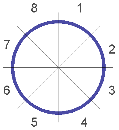 the thick blue line represents the CRT beam. The octants are numbered so the capital letter "C" is drawn using octants 1, 4…8
with the beam on and with the beam blanked for 2 & 3. I'll do one more complete example, the numeral "5":
the thick blue line represents the CRT beam. The octants are numbered so the capital letter "C" is drawn using octants 1, 4…8
with the beam on and with the beam blanked for 2 & 3. I'll do one more complete example, the numeral "5":
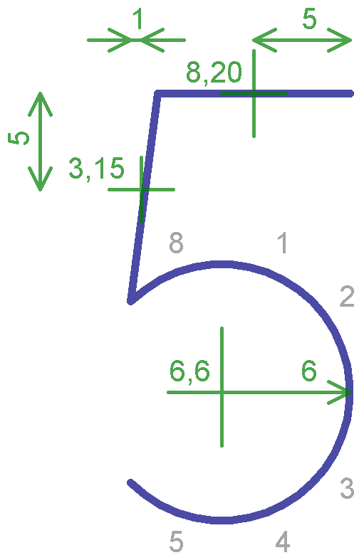
This diagram shows that this rather smart 5 is made up of three objects:
- A horizontal line (X=8, Y = 20, A = 0, B = 5)
- A positive slope line (X = 3, Y= 15, A = 5, B = 1
- An arc (X = 6, Y = 6, A = B = 6, drawing octants 1 … 5 & 8
In each case X and Y are the objects centre coordinates (fixed offsets) and A and B are the X and Y magnitudes (size = radius)
Bringing it together
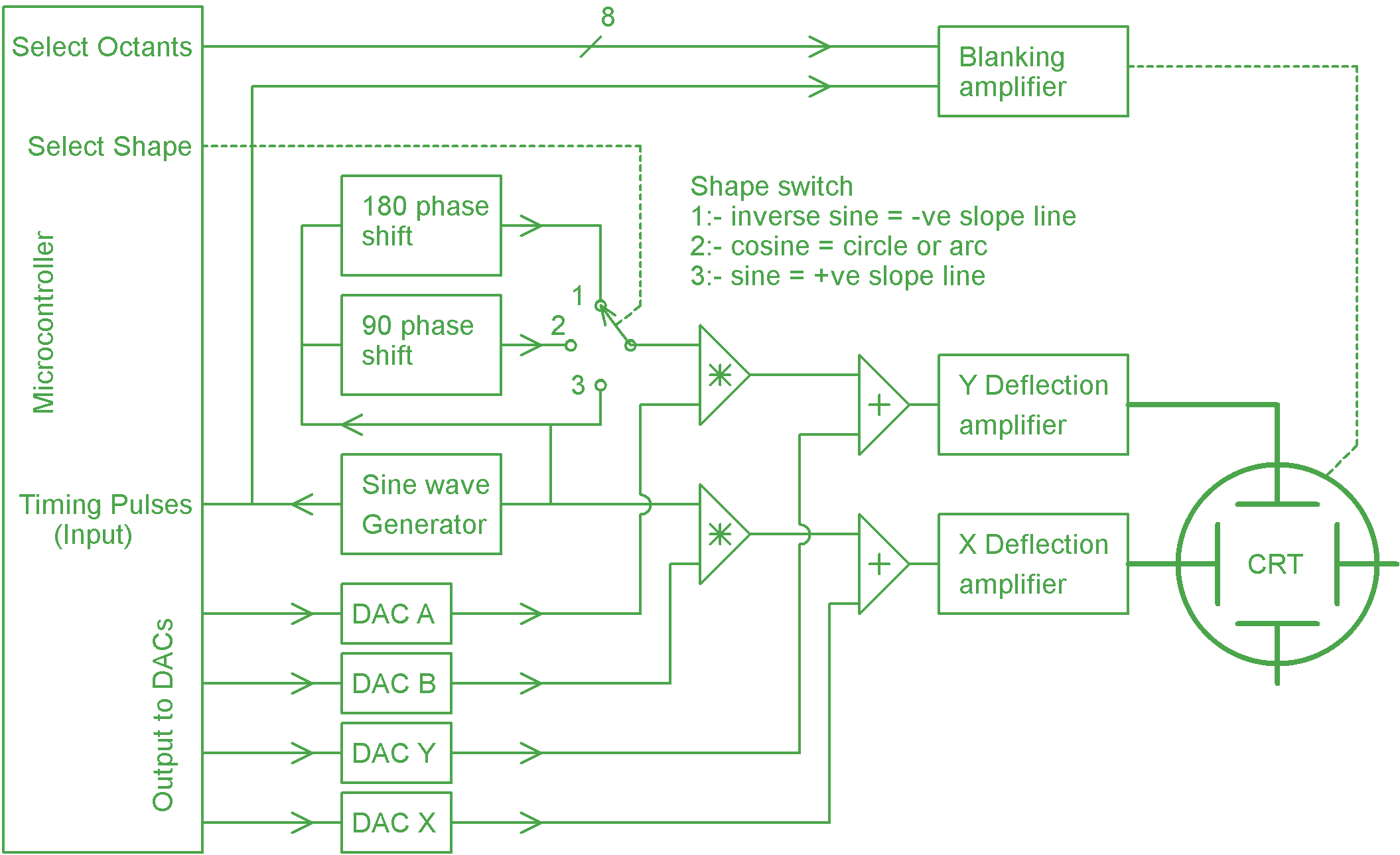
This block diagram shows how the requirements given in the last section can be brought together as a step towards the hardware and software design. At this point in the description, I need to flip the x and y axis equations over as the hardware uses a sine wave only on the x-axis and the selected equation wave on the y-axis. It makes no difference but the discussion and equations presented so far were compatible with the animation from the wiki but at 90° to the actual hardware.
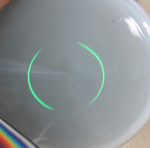
The heart of the circle drawing circuit is the sine wave generator the stability and purity of this sine wave will have a marked effect on the quality of the objects drawn. Harmonics and digital noise are both unwelcome and will produce flat sides or wiggles in the curves or fuzz or wider than necessary beam width. This was an early experiment with a sine/cosine generator - no way good enough! Noise from the power supply:
Noise has gone - but look at the bumps and flats! Too much harmonics are present:
Ok, nearly there…
~$%@#=?%$ blanking amplifier is not fast enough!
Remembering that the general equation for the x-axis is (now) x = X + Bsin(φ), our sine wave is fed to the X deflection amplifier first through a multiplier (shown by * symbol) where it is multiplied by the output from DAC B, and then through and adder (symbol +) where the output from DAC X is added.
The Y axis is slightly more complex as three equations are used:
- y = Y + A × sin(φ + π) for straight lines with a negative slope which is obtained by shifting the phase of the sine wave by 180°
- y = Y + A × cos(φ) for circles and arcs which is obtained by shifting the phase of the sine wave by 90°
- y = Y + A × sin(φ) for straight lines with a positive slope which is obtained by using the sine wave unchanged
In exactly the same way as the x axis, the selected y waveform is first multiplied by the output from DAC A and then an offset is added from the output of DAC Y.
The blanking amplifier receives 8 bits of information, each bit specifying one octant to light. For synchronisation purposes, it also receives a timing signal from the sine wave generator so that the blanking signal to the CRT is switched at exactly the same point during each circle orbit so only full orbits are drawn.
If the sine wave generator is the heart, then the microcontroller is the brain (this is an awful analogy, sorry). To display a single object, the microcontroller must execute this procedure:
- The selected octants value is set to zero so no octants are displayed - the CRT is blanked
- Position the shape switch to select a -ve line, circle or +ve line
- Send the Y size to DAC A (may be zero if a horizontal line is being drawn)
- Send the Y position to DAC Y
- Send the X size to DAC B (may be zero if a vertical line is being drawn)
- Send the X position to DAC X
- Wait for a sine wave timing pulse so that the beam is at a known position in its orbit
- Send the 8 bit octant information to the blanking amplifier, the CRT lights up!
- Count the number of timing pulses received so that the object is displayed for the correct amount of time, i.e. number of orbits, to give the required brightness.
- Finally, set the 8 octant bits back to zero to blank the CRT.
Congratulations, one object has been drawn! This process is repeated for all the objects to fully draw the image on the CRT. When all the objects have been drawn the whole process is repeated at a rate to give a flicker free display (say 50 or 60 times a second).
Simplified Schematic
This section shows a simplified view of how the hardware block diagram is implemented with two Atmel AVR's, a quad DAC, an analogue switch and five opamps. After this the other clock circuits such as the chimes generator and RTC will be shown simplifed.
Sine, Cosine and Inverted Sine Generation
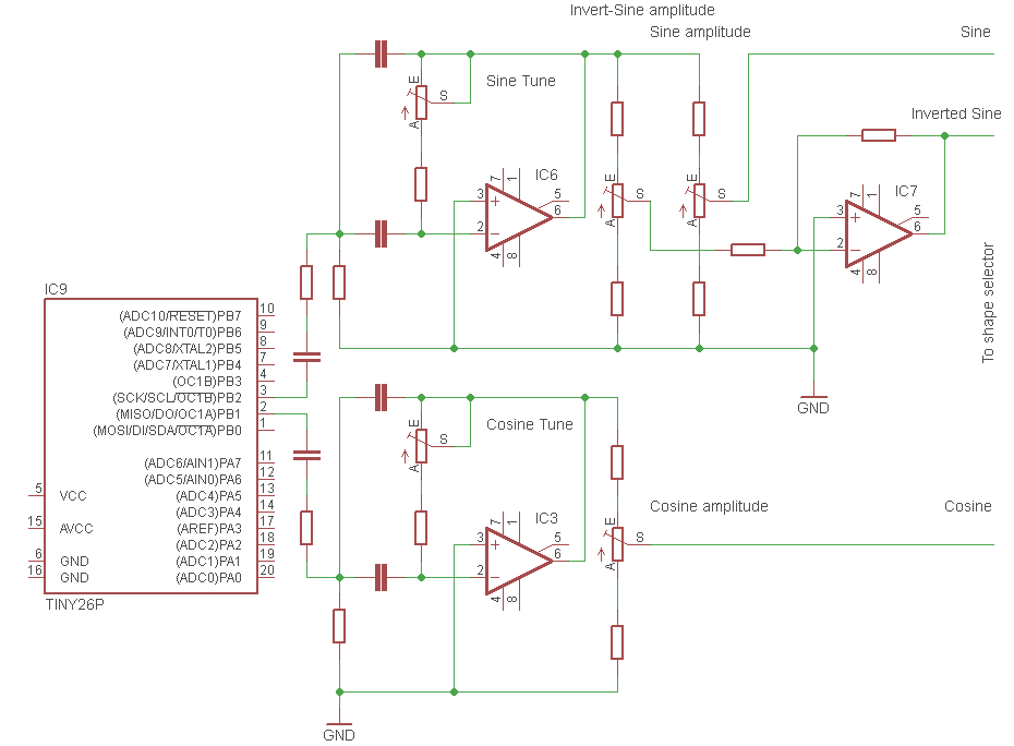
IC9 is an Atmel attiny26, the firmware contains the sine wave oscillator (although at this stage the output is, of course, a squarewave) at about 32kHz and is the basis of all the circle drawing timing. (The oscillator in the firmware actually runs at 8 times this frequency, about 256kHz, and is divided in the firmware to produce the required outputs.) The "squared" sinewave is output on PB2. The attiny also contains the 90° phase shifter to produce a "squared" cosine on PB1. These signals look like this (on a Rigol DS1052E):
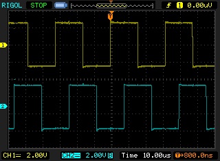
Each of these signals is passed into an opamp based band pass filter. These filters, IC3 for the cosine signal and IC6 for the sine signal, have a fairly high Q and can be finely tuned to the squared fundamental frequency. These opamp bandpass filters invert the signal so an input squarewave and output sine wave looks like this:
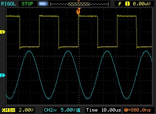
and the two extracted fundamentals are:
The sine wave is inverted by another opamp, IC7, so we now have our three signals: sine, cosine and inverted sine which are passed to the shape selector.
Shape Selection
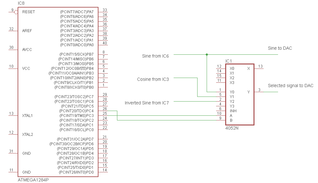
The sinewave from IC6 passes to input Y0 on IC1 which is a 4052 four channel multiplex analogue switch, IC6 takes the cosine signal on input Y1 and the inverted sine on input Y2 (input Y3 is unused). Which signal is selected is set by the A & B inputs, these are taken from PC3 and PC4 on the main controller, an Atmel atmega1284p. The sinewave from IC6 and the selected shape signal from the Y output of IC1 are passed to two of the DACs.
Signal multiplication and offset addition
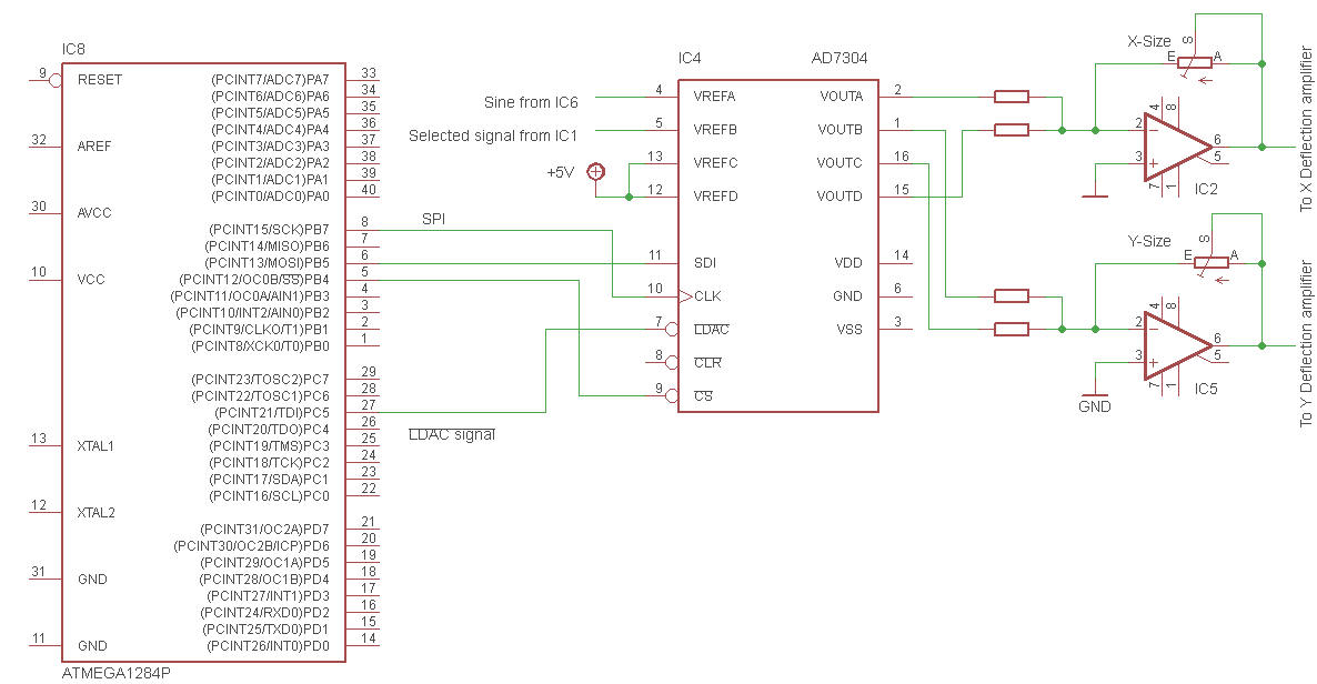
IC4 is a AD7304 quad multiplying DAC and carries out the functions of DAC A, B, X and Y, and the signal multiplication shown in the block diagram. The sine wave from IC6 feeds VREFA (DAC A reference voltage input) on IC4. The output from the shape selector switch, IC1, goes to the VREFB input on IC4. The outputs on pins VOUTA and VOUTB will be the input sine wave and selected wave multiplied by the value loaded into the respective DAC. The outputs VOUTC and VOUTD have their corresponding reference inputs VREFC and VREFD tied to 5V so the outputs provide the X and Y offset voltages. The multiplied signal and offset are added together in IC2 for the X deflection and IC5 for the Y deflection respectively. The AD7304 DACs are buffered, so the four values are loaded using the SPI bus, and then the LDAC line from IC8 PC5 is toggled and the four DAC values are brought into to use simultaneously. This completes the description of how the x and y deflection signals are created.
Brightness control and blanking
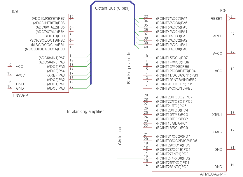
Brightness control is made by counting the number of orbits the beam makes; at the start of each orbit a pulse is sent from PB3 on IC9 (the attiny) to PD2 on IC8 (atmega). PD2 is also an external interrupt pin so the handling of the counting pulses can be made using an interrupt triggered function in the firmware. The pulse occurs at the same point in each orbit so the the drawing functions in IC8 can remain synchronised with the circle drawing.
Blanking is achived by two methods, first as described above, an 8 bit octant bus sends the required octants to light or blank from Port A on IC8 to Port A on IC9. Complete blanking can be achieved by setting the octant bus to zero. A second method (not described above) is an override signal from PC7 on IC8 to PB6 on IC9. This overrides the octant bus value and blanks the CRT completely. Using this single control line has the advantage that it does not disturb the current octant bus value. Synchronisation of the circle orbit and the CRT blanking is carried out in the firmware in IC9. The final blanking signal is sent from PB0 on IC9 to the blanking amplifier. A logical 1 makes the beam visible and a logical 0 blanks the beam.
Complete Simplified Schematic
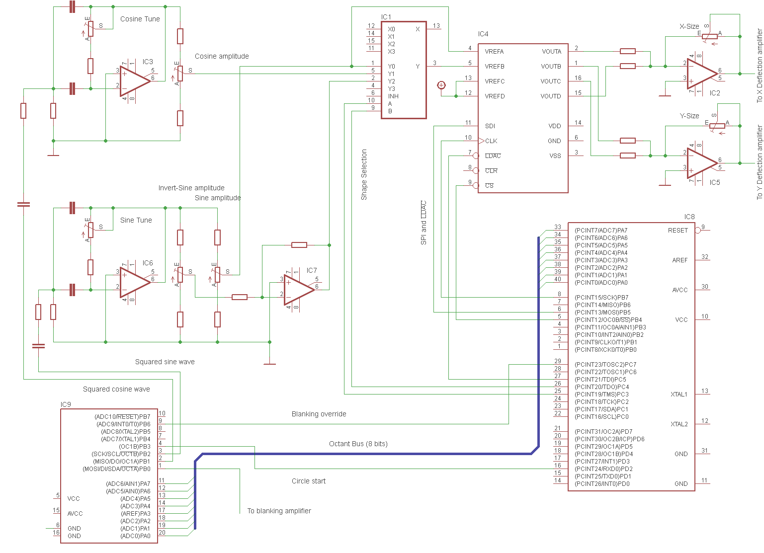
All the the schematic extracts above are combined here into one simplified schematic. The software for the two AVR's is in the zip files in the software section above.
The Mundane Part
To function as a clock more than just the circle drawing parts must exist. These simplified design notes cover:
- The chimes sounder
- The real time clock
- Deflection amplifiers
- The blanking amplifier
- Miscellaneous services - main sychronisation, rotary encoder, LED and UART
- Power supply requirements
Chimes
The chimes are generated by a SAE800 gong chip and is probably worth a special mention as it is a simple way to get single, dual or triple gong tones. In the triple tone mode the notes, for example can be arranged as the minor and major third: e2 - c# - a, corresponding to 660Hz, 550Hz and 440 Hz.


The gong chip allows the tone fundamental frequency and volume to be adjusted by setting two resistor values. Here is a recording with the camera microphone of the gong chip in action:
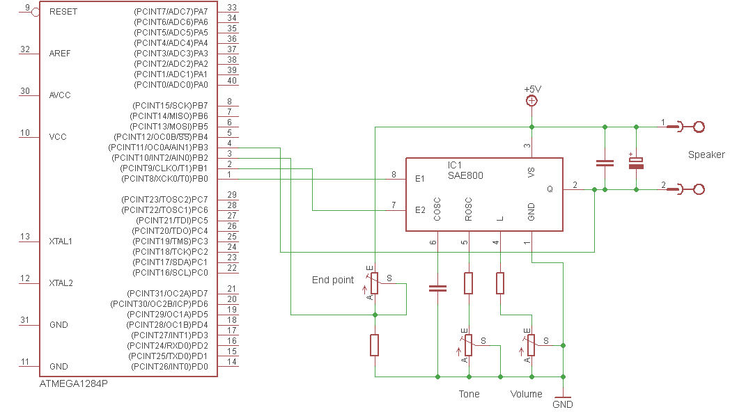
This simplified schematic shows how the SAE800 is connected to the atmega. In principle, only two connections are required to the enable inputs (E1 and E2 pins, here connected to PB0 and PB1) but there is a problem with the SAE800 in this application. The SAE800 cannot be retriggered to produce another tone sequence until the current tone sequence has finished. I detect the tone completion using the atmega's analogue comparitor as the output voltage (Q) rises to 5 volts when the tone sequence is finished. The output from the SAE800 goes to the AIN1 input (PB3) and an adjustable reference voltage goes to the other comparitor input AIN0 (PB2). The quality of the sound is very dependant on the quality and size of the speaker used.
Real Time Clock (RTC)
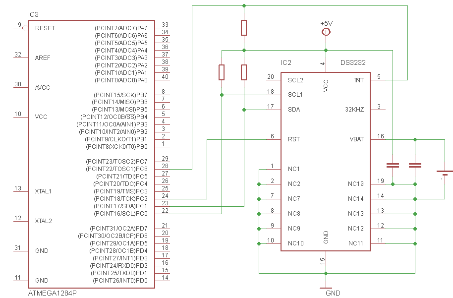
It says on the tin The DS3232 is a low-cost temperature-compensated crystal oscillator (TCXO) with a very accurate,
temperature-compensated, integrated real-time clock (RTC) and 236 bytes of battery-backed SRAM. Additionally, the
DS3232 incorporates a battery input and maintains accurate timekeeping when main power to the device is interrupted.
The integration of the crystal resonator enhances the long-term accuracy of the device as well as reduces
the piece-part count in a manufacturing line.
The DS3232 uses an i²c (Atmel TWI) interface and so its SCL and SDA pins simply connect to the SCL and SDA (PC0 and PC1) on the atmega. The DS3232 interrupt output (which is programmed to 1Hz) is connected to PC6 and the reset pin is connected to PC2. A battery is provided to keep the device running when the clock is switched off.
Deflection amplifiers
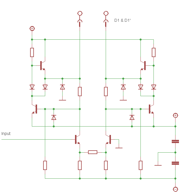
There are two of these amplifiers; they are a straight copy with no changes whatsoever from the design used by David Forbes.
Blanking amplifier
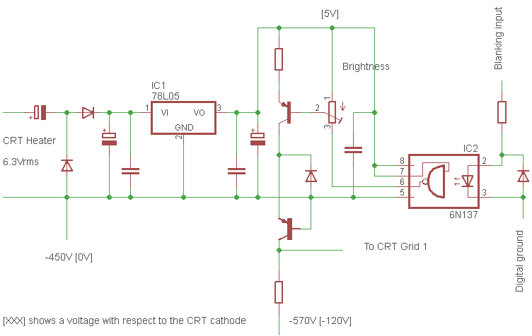
A straightforward design not unlike the one used in my first scope clock. Except I noted that David Forbes used an opto isolator between the blanking amplifier and the digital electronics - I copied this. The blanking amplifer "ground" is the CRT cathode potential which is at -450V to ground and earth in the clock. The blanking amplifer also requires -570V (-120V with respect to the cathode) to full blank a DG7/32 CRT. The amplifier also requires a small positive voltage which I borrowed from the CRT heater supply.
Miscellaneous services - main sychronisation, rotary encoder, LED and UART
The last few odd 'n' sods are brought together on port D of the atmega:
- The atmega UART0 is unused brought out to connection pins along with ground and 5V. This is to allow future addition such a GPS module or a serial link to a PC. Pins D0 and D1 are otherwise unused.
- A rotary encoder with a push button is conected to D4, D5 and D6. This is the only user control and is used to choose the clock face to display, navigate the menu system and edit menu items.
-
An AC signal is taken from the low voltage power supply, heavily filtered and clipped using the atmega's input protection diodes.
The signal on pin D3 looks like this:
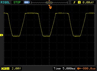 Pin D3 is an external interrupt pin and this signal is used to start the CRT refresh cycle. So it starts every 20mS with 50Hz mains
and 16.66mS with 60Hz mains. Being synchronised to the mains prevents moving distortion or "swimming" of the image due to external
magnetic fields. It is fast enough to prevent any flicker on the DG7/32, which has a short persistence phosphor, but is does mean
that the screen refresh must have been completed in this time period which limits the number and size of the objects that can be drawn.
But as you have seen above, this has not proved a problem.
Pin D3 is an external interrupt pin and this signal is used to start the CRT refresh cycle. So it starts every 20mS with 50Hz mains
and 16.66mS with 60Hz mains. Being synchronised to the mains prevents moving distortion or "swimming" of the image due to external
magnetic fields. It is fast enough to prevent any flicker on the DG7/32, which has a short persistence phosphor, but is does mean
that the screen refresh must have been completed in this time period which limits the number and size of the objects that can be drawn.
But as you have seen above, this has not proved a problem.
- Lastly, pin D7 connects to an LED for debug purposes. A jumper can isolate the LED when not required.
Power Supplies
The power supplies are extensive as many voltages are required to drive the CRT, the analogue electronics and the digital electronics. I used (see parts list for full details) two transformers to get all of the voltages and I also provided separate rectification and stabilisation for the digital and analogue circuits so that digital crud didn't find its way into the analogue outputs. These are the voltages and purposes:
- 240V deflection amplifier HV supply
- 120V CRT final anode supply
- 0 - 80V variable CRT focus anode
- 6.3V AC CRT heater
- -450V CRT cathode
- -570V CRT control grid
- 5V DC (with respect to the CRT cathode) blanking amplifier
- ±12V and ±5V analogue supply
- 5V digital supply
But, when all said and done, its just a bunch of diodes, capacitors and stabilisation ICs. I have left you to look at the detailed schematics to find the PSU elements; they are not centralised but implemented where they are required.
Afterword: no PDA supply is included here as the DG7/32 doesn't have one. But the high voltage AC is brought to header pins so that an additional PCB carrying a multiplier chain to get the few kV needed is provided.
Quick Links