
Retro look as well…

Introduction
In the 1970s I worked for a while for the UK Atomic Energy Authority (UKAEA) at a site in Winfrith, Dorset. Amongst a lot of other interesting work, I used a gamma ray density gauge that amounted to a caesium-137 source, in its castle and collimator, the target (various), a sodium iodide detector (from memory), a photomultiplier and a series of counters using dekatrons. Having spent hours taking readings off the dekatron counters I somehow still associate dekatrons with things "atomic1"…
Precision frequency generators using the rubidium atomic frequency standard have been around for many years; second hand units have found there way on to Ebay at modest (circa $100 US) prices. I have built a number of clocks of varying accuracy - time set using Internet time standards, time set by GPS and using a humble crystal oscillator. So an alternative would be to use a clock based on a Rubidium atomic frequency standard. This would have the small advantage of being accurate (once set) without requiring external intervention (as the Internet and GPS clocks require).
Having seen other "atomic1" nixie clocks (nixiebunny and jthomas as examples) it perhaps came naturally (to me anyway) to use dekatron as the clock display. Dekatrons are not as common as nixies in clocks using glowing neon but examples are around on the net (Bill (about a 3rd down the page), Jason Harper).
Lastly, I wanted a clock with as many switches, buttons and lights as I could manage (as against imagine which could be a nightmare).
Revision history (February 2010 - December 2012)
The first version of this clock I built during 2008 with these webpages first published in February 2009. During the last few year I have tinkered with the clock to resolve a few hardware problems. The main changes have been to
- work with both 50 and 60Hz mains frequencies
- improve the chime sequence repeat rate
- improve the high voltage switching arrangements
- allow Russian OG4 dekatrons as well as orginally GC10B dekatrons to be used
- giving the software a complete workover to make it more robust
- write a series of test programs so individual subsystems could be independantly and fully tested
- replace the front panel with a laser cut/engraved one
- rewrite the software using the free GCC-AVR C Compiler
These changes have resulted in the divider and main microcontroller boards being first adapted and eventually replaced and a few trivial changes to the interboard wiring. Only the new boards and their software will be described below the legacy cards are all abandoned although the old front panel design is still available (within the Eagle file download).
In reworking this webpage I have also added more information on the construction and front panel wiring.
The divider card software, dekatron card software, test software and final clock software are all now available for download.
Atomic Clock
The rubidium oscillator I bought on Ebay is a Datum LPRO.

Internally the oscillator operates as follows:
A microwave signal is derived from a 20MHz voltage-controlled crystal oscillator (VXCO) and applied to the rubidium (Rb 87) vapour within a glass cell. The light of a rubidium spectral lamp also passes through this cell and illuminates a photo detector. When the frequency of the applied RF signal corresponds to the ground-state hyper-fine transition of the Rb87 atom, light is absorbed, causing a decrease in the photo detector current . The dip in photo detector current is used to generate a control signal with phase and amplitude information which permits continuous atomic regulation of the VXCO frequency. The VXCO signal is divided by 2 and fed through a buffer amplifier to provide the standard frequency output of 10 MHz.
To me it is just a "black box", feed it correctly and it produces a precision 10MHz sine wave. It does produce some other diagnostic signals to show the unit is healthy:
-
BITE Built In Test Equipment signal to show the VCXO is locked to the atomic transition. As long as BITE is low once the unit has warmed up,
the output frequency is within roughly ±5E-8 of absolute frequency.
-
LAMP V signal monitors the inherent degredation of the lamp light pickup; this signal should be >3 volts and < 14 volts.
- XTAL V MON signal can be used to show if the crystal is drifting out of the available trim range; this signal should be > 0.55 volts and < 12.6 volts.
When I hooked a power supply up to the second hand unit, I was pleased to find the BITE signal when low after a few minutes (lock achieved) and the LAMP and XTAL voltages were both roughly mid range (in my ignorance I assume this is good).
By "feed it correctly" the LPRO requires a 24v peak 1.7A, normal 0.5A; power supply. The clock requires more than a 10MHz oscillator so I originally decided to use the a PCF8583 clock chip. This chip will accept a 50Hz signal (so I need a divide by 200,000 to get 50 Hz from 10 MHz) and communicates with a microcontroller using TWI (I²C) interface. I decided to pinch the nixiebunny idea of using batteries to preserve clock operation during power loss. The batteries would be float charged but capable of running the rubidium oscillator (0.5A at 24V) and the miscellaneous divider chain and clock. Then a thought occurred - why not measure time using mains frequency in a second PCF8583 clock chip so that absolute and long term differences between "mains" and "rubidium" could be measured. This arrangement has one disadvantage - there is no 60Hz mains version of the PCF8583 available and I have received interest from LandOf60Hz in replicating the clock. So I kept the legacy of dividing 10 MHz to 50 Hz (as I explain below I needed to divide to 1 Hz anyway) but swapped the two PCF8583 clock chips with a single ATMEGA168 to count transitions from the divider chain or from filtered mains and to communicate the count using a TWI interface. (On the way I considered using something like a ATTINY13 programmed as a "60Hz" PCF8583 but this seemed an overly complex solution.)
In the UK mains frequency is 50 Hz but does drift either side but is governed so that the average is 50 Hz (see here), for example, 60 minutes of data look like:

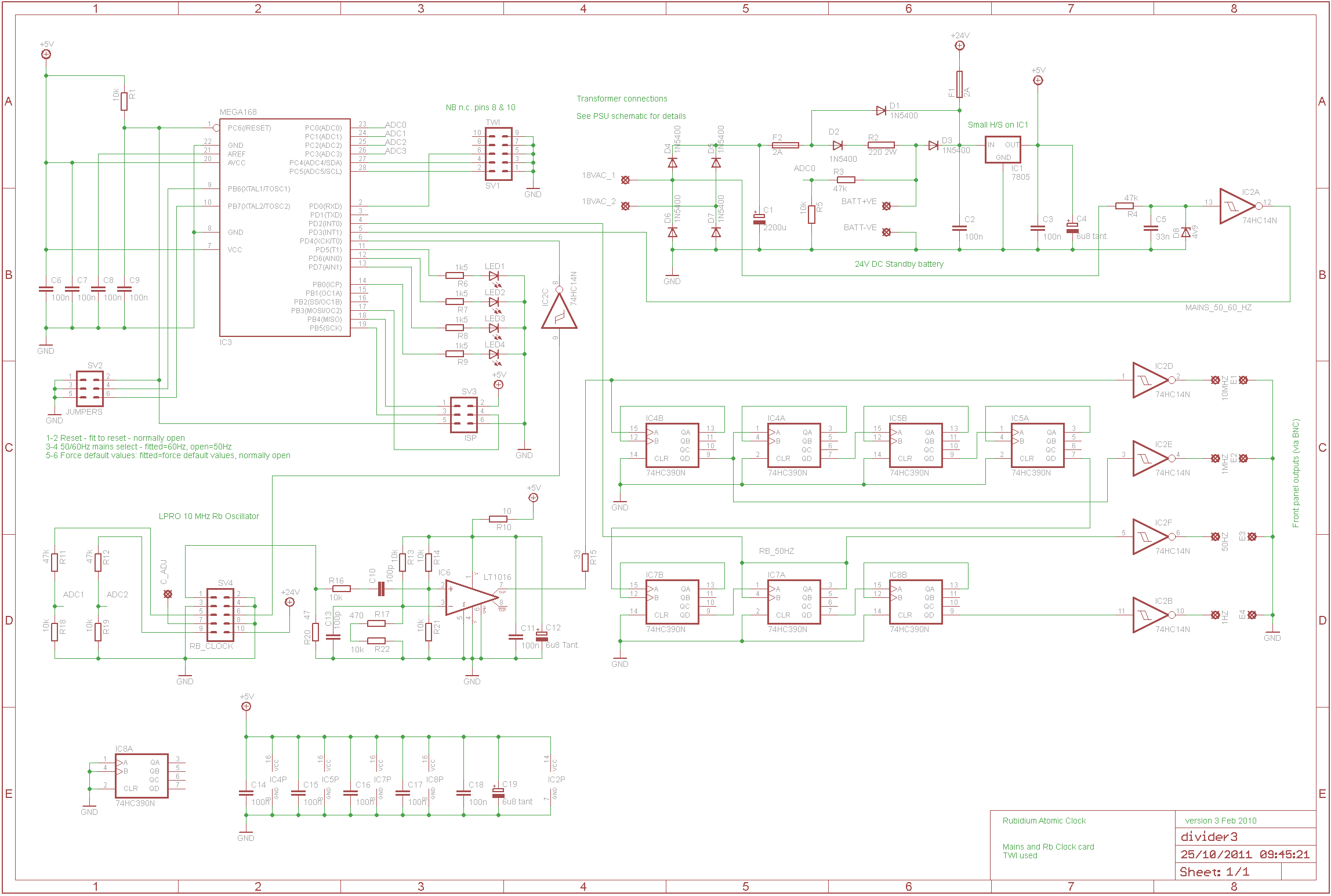
Finally, I wanted front panel outputs of the various frequencies available down to 1 Hz (so the divider chain would be divide by 10,000,000 in total). The first PCB for the clock was now evolved:

- 24 VDC and 5 VDC power supply
- Mains (float charged) battery
- 10 MHz buffer (design from LPRO manual using a LT1016 fast comparator)
- Divide to 1 Hz in a series of divide by 2 divide by 5 steps (74HC390)
- Buffered outputs at 10 MHz, 1 MHz, 50 Hz, 1 Hz
- ATMEGA168 chip linked (interrupt) to rubidium 50 Hz divider output and linked to filtered and squared 50/60 Hz mains frequency
- Sensing BITE ("locked"), LAMPV ("lamp"), XTAL V MON ("crystal") signals by the ATMEGA168
- TWI link to the main microcontroller (clock counts, sensed values)
- 1 Hz interrupt from the Rb oscillator derived clock
- LEDs to indicate oscillator lock (BITE low), 1 Hz pulses from the two clock sources and an error status
- Off board would be a 18 + 18 VAC 50VA torriodal transformer
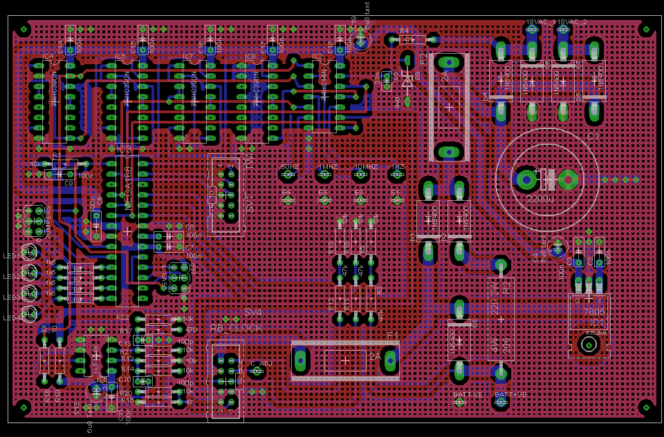
Divider Schematic and PCB layout
Right click and then "save as" to see these images at higher resolution. The board Eagle files are available for download below. I built the board up first and tested it with an ATMEGA32 based test card to check the mega168 clock could be addressed and that all of the required signals were available. Everything was OK so I moved on to the dekatron display cards.
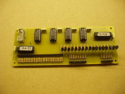
Dekatron Display

© GIF created by Dieter Waecher

In electronics, a Dekatron (or Decatron, or generically three-phase gas counting tube or glow-transfer counting tube or cold cathode tube) is
a gas-filled decade counting tube. Dekatrons were used in computers, calculators and other counting-related devices during the 1940s to 1970s.
The dekatron was useful for computing, calculating and frequency-dividing purposes because one complete revolution of the neon dot in a dekatron
means 10 pulses on the guide electrode(s), and a signal can be derived from one of the ten cathodes in a dekatron to send a pulse, possibly for
another counting stage. Sending pulses along the guide electrodes will determine the direction of movement.Internal designs vary by the model
and manufacturer, but generally a dekatron has ten cathodes and one or two guide electrodes plus a common anode. The cathodes are arranged in a
circle with a guide electrode (or two) between each cathode. When the guide electrode(s) is pulsed properly, the neon gas will activate near the
guide pins then "jump" to the next cathode. Pulsing the guide electrodes repeatedly will cause the neon dot to move from cathode to cathode. The
dekatron fell out of practical use when transistor-based counters became reliable and affordable. Today, dekatrons are used by electronic hobbyists
in simple "spinners" that runs off the mains frequency or as a numeric indicator for homemade clocks.
To operate the dekatrons you need several things:
- High voltage for the anodes (typically 375 - 400 volts above the cathode voltage)
- An intermediate voltage to hold the guide electrodes positive with respect to the cathodes
- A means to take the guide electrodes to a voltage much lower than the cathodes so that the glow is transferred on to it
- A means of detecting that cathode zero is glowing
This circuit shows the principles (from an original design by Mike Moorrees):
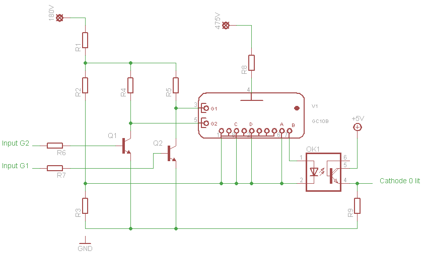
The cathodes are held a a positive voltage with respect to ground (this will avoid requiring a negative supply). A signal on one of the two inputs will bring the guide electrode down to a voltage negative with respect to the cathodes and so the glow will transfer onto that guide. Sequencing the pulses onto the two inputs will make the glow rotate in either a clockwise or anti clockwise direction. When cathode zero is glowing (B output on a GC10B dekatron) the cathode 0 lit output will go high.To rotate the glow the following sequence is needed:
- Starts with inputs G1 and G2 both low
- Make Input G1 high
- Wait a few 100 μS - dekatrons are relativily slow - glow moves to G1 electrode adjacent to the glowing cathode
- Make Input G2 high
- Wait a few 100 μS - glow becomes "shared" between the two guide electrodes
- Make Input G1 low
- Wait a few 100 μS - glow moves to G2 electrode
- Make Input G2 low - restoring the original state
- Wait a few 100 μS - the glow moves onto the cathode adjacent to the G2 electrode
- Success - the glow has moved from one cathode to another!
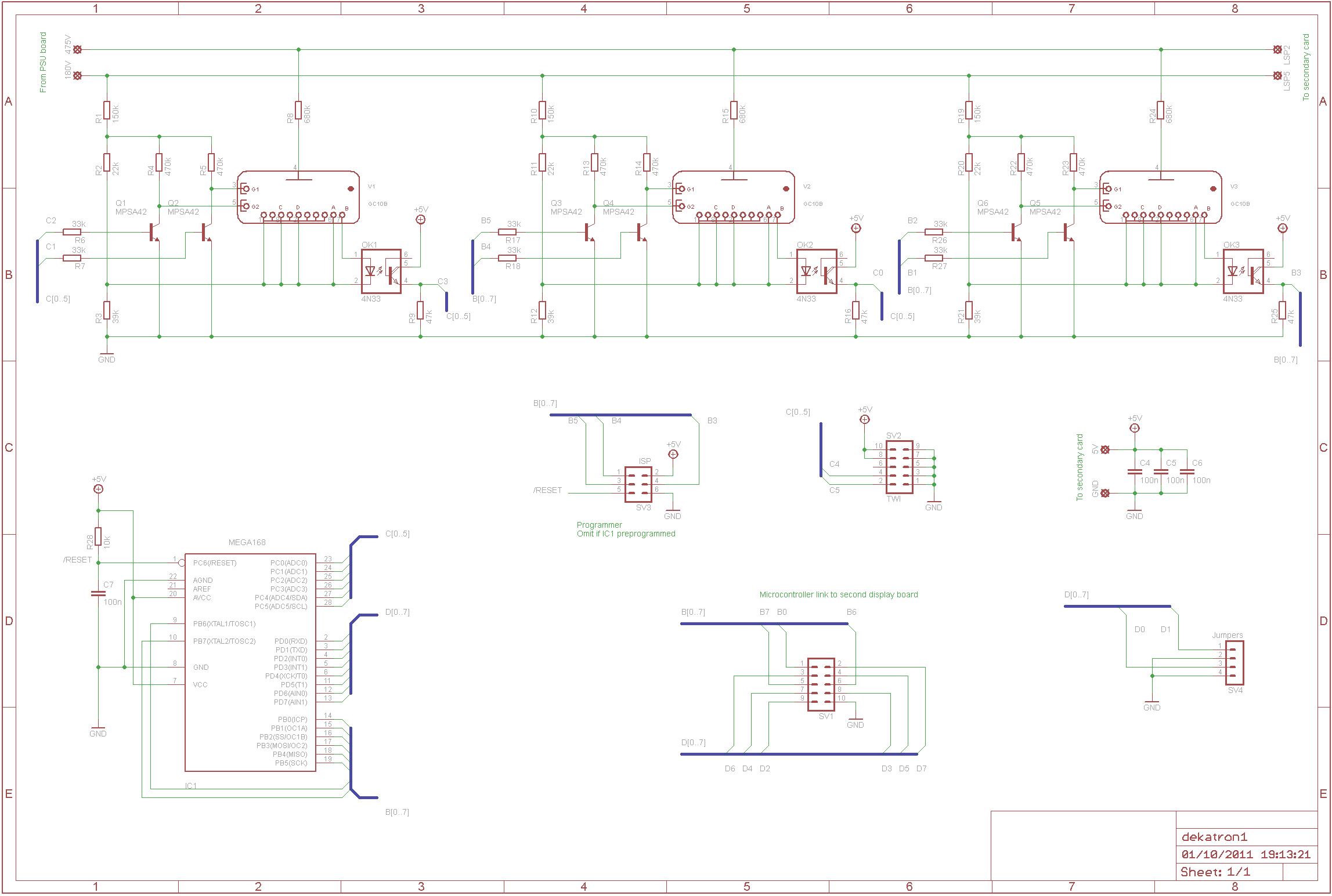
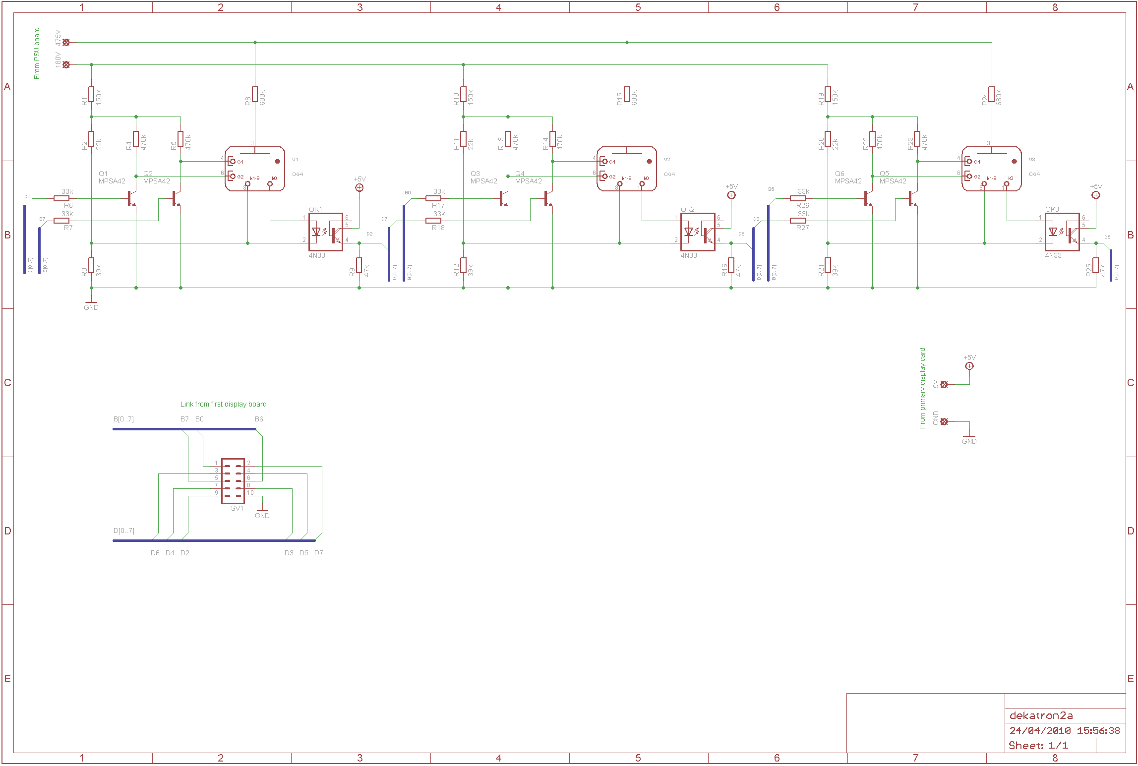
By sequencing the guide electrodes in the opposite order (G2 first) the glow will rotate in the opposite direction. Since on start up the cathode that glows first is unknown it is simple to rotate the glow using this sequence until a high is detected on the cathode 0 lit output; the dekatron is now in a known state (zero).So six dekatrons (hours : minutes : seconds) requires 12 outputs and 6 inputs from a micro controller. This is fairly heavy demand of I/O pins if I was using a single ATMEGA644P (as intended) which has 32 I/O pins. Since I was already using an TWI interface for the clock chips it seemed logical to look at using TWI port expanders. The PCF8574 expander has 8 I/O pins so irratingly I would need 3 chips. An alternative was to use, say, an ATMEGA168 as an TWI slave. This chip can be arranged to have upto 23 I/O pins - I need 18 for the dekatrons, 2 for the TWI, 1 for the reset (so I can use my usual programmer) and that makes 22 pins used - with 2 spare. I will use the internal 8 MHz RC oscillator which is good enough for this application. I use the "not for profit" version of Eagle which limits me to 160 x 100mm boards. To space the 6 dekatrons out sufficently I needed to space the design across two PCBs (which I actually cut to 150 x 100mm). An early design arranged the dekatrons in a 3 x 2 pattern rather than the straight 6 used here - I din't like the resulting front panel designs, although the dekatrons the fitted onto a single 160 x 100 mm board. Links connect the first and second boards together. The ATMEGA168 is on the first board. The software would configure the ATMEGA168 as a TWI slave, would handle all the glow movements and accept commands like "move glow on dekatron 3 to position 2". This would only take 2 bytes on the TWI bus. Other commands would set all glows to position zero (1 byte), set all 6 dekatrons to given positions (7 bytes) and also to force the ATMEGA168 to reset (1 byte). This all looked simple enough but I made the data structure more complex by adding a simple CRC7 checksum to make the communication more robust. This added a single byte to each command.
One spare input pins is arranged to put the card into a self test mode if grounded (eventually I may to use the second pin for some purpose).
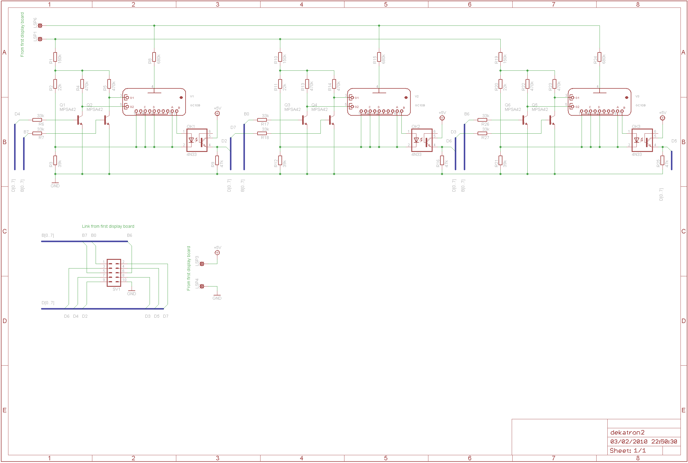
GC10B version

Note the orientation of the octal sockets so that pin 6 is uppermost. This pin corresponds to cathode 0 which will then be at the top.
OG4 version
I have also produced a version of the cards to use the Russian OG4 dekatron which are currently in more plentiful supply than GC10/B dekatrons. The OG4 supply (on EBay, at the time of writing this) is for NIB dekatrons whereas the GC10B available tend to be (well) used - often electrode zero is entirely eroded away.
Note the orientation of the octal sockets so that the spline is uppermost. This pin corresponds to cathode 0 which will then be at the top.
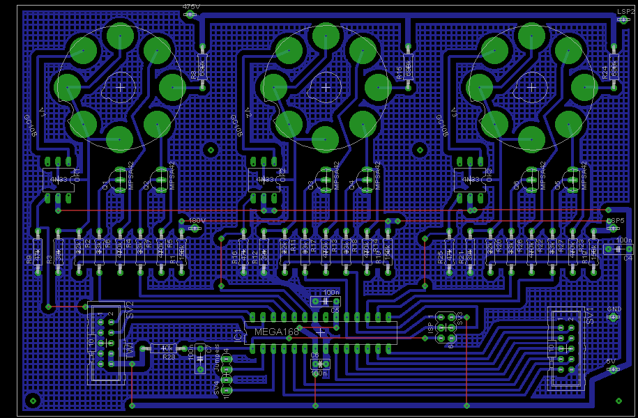
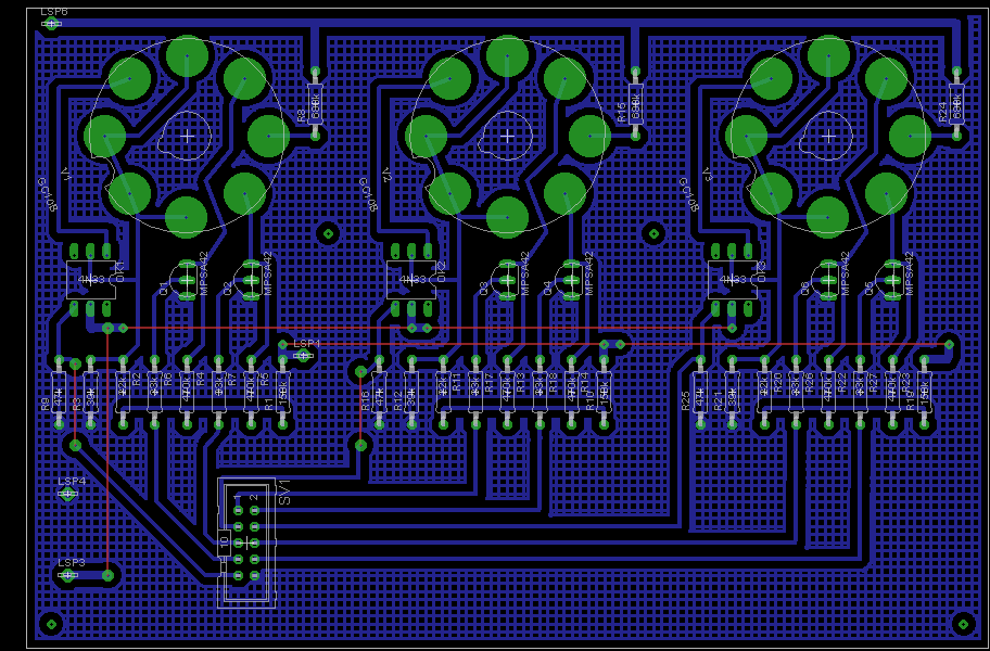
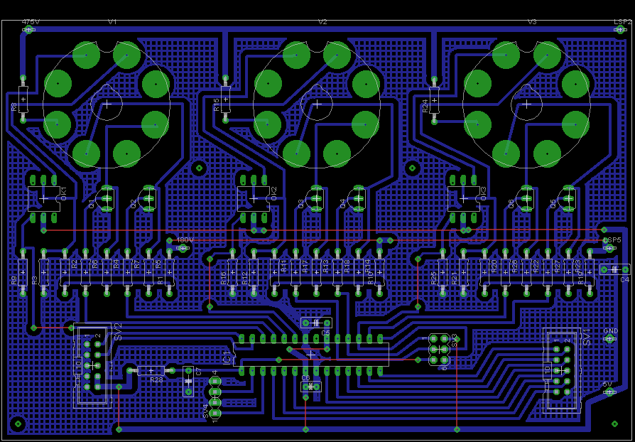
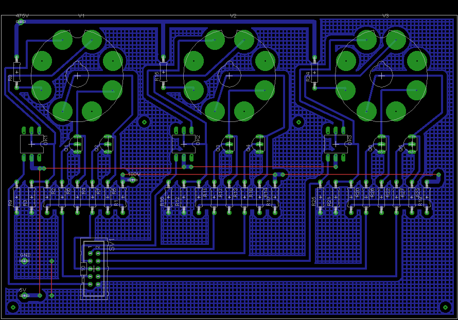
Dekatron Schematic and PCB layout
Right click and then "save as" to see these images at higher resolution. The board Eagle files are available for download below.
GC10B version:
OG4 version:
To test this board I now needed the main clock power supply that would deliver 475V, 180V and 5V. So I'll describe this next.
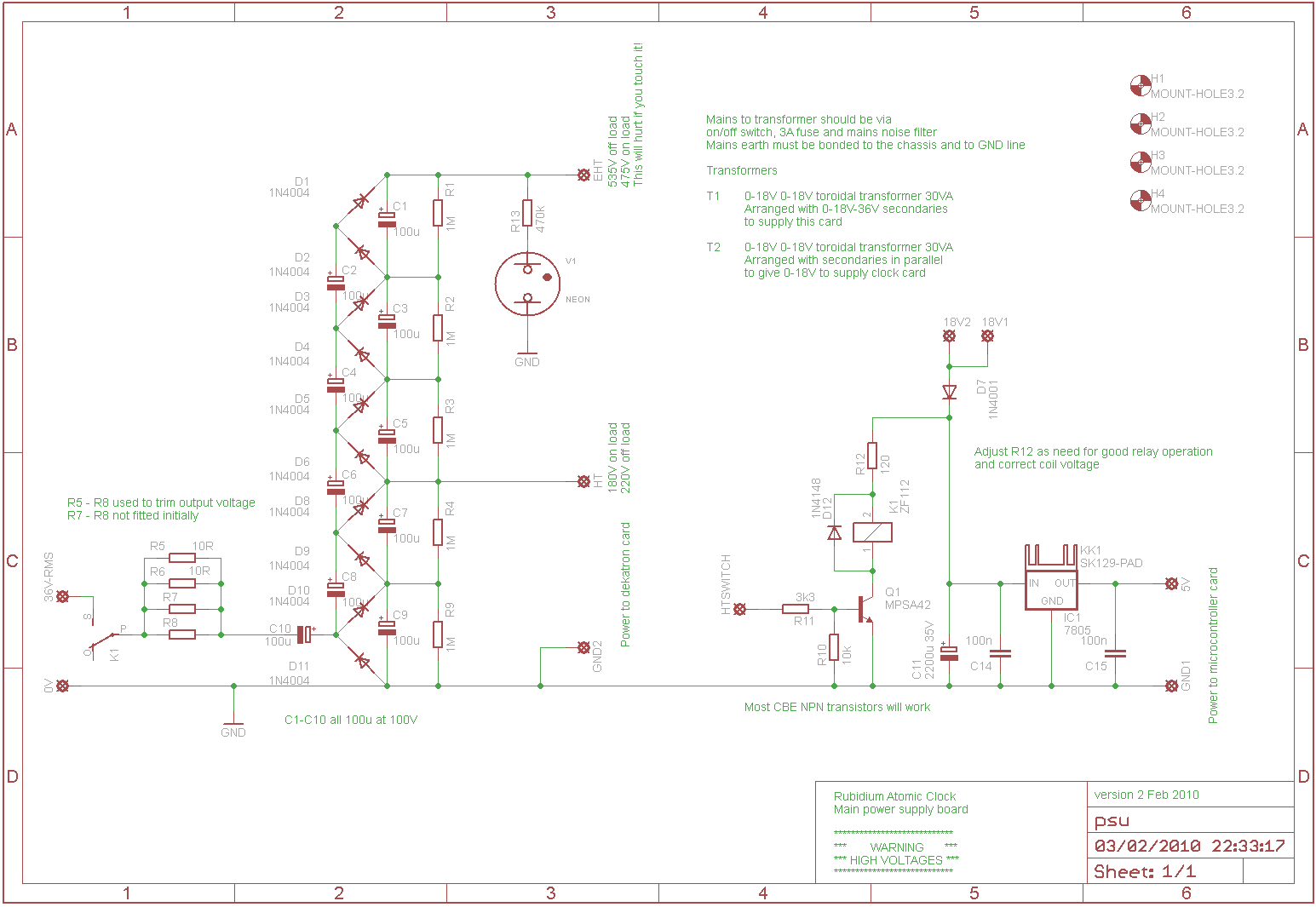
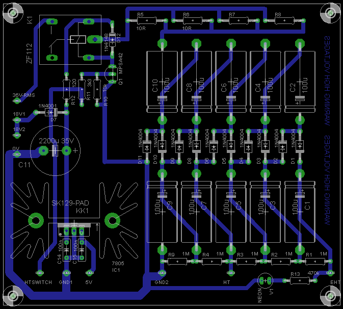
Main Power Supply
I chose to use the same power supply I had used successfully with the bookcase clock that used a dekatron as well as four nixies. This would deliver the required voltages for the remainder of this clock when using a 15VA 18-0-18 VAC torroidal transformer. The power supply is physically large compared with other designs but I have plenty of space in the case I planned to use (more on the case selection and final assembly below).
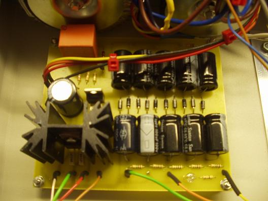
I wanted to be able to turn off the dekatrons (to extend their life) when the clock was not in use but leave the rest of the clock running. I therefore added a relay to switch the AC feed into the voltage multiplier. I added a neon bulb as a warning indicator when the multiplier held a charge: touching the 475 V supply would smart to say the least… Not much else to say about power supply other than I added an on/off switch and fuse on the mains side of the two transformers together with a small (3A) LC filter to remove any rubbish on the mains. QED.
Main Power Supply Schematic and PCB Layout
Right click and then "save as" to see these images at higher resolution. The board Eagle files are available for download below.
Front Panel IO
The penultimate card is the front panel I/O. This uses four PCF8574 8 bit TWI I/O expanders to give 32 control lines. Since I was planning on a large number of front panel switches and neons I knew I was going to go beyond the I/O capabilities of the micro controller I planned to use. An alternative would be to use a third microcontroller as another TWI slave but I have a tube of PCF8574 chips available and they would provide the required I/O together with an interrupt signal to the main microcontroller when a switch was moved so I would not have to poll all of the switches in the software to detect changes. The main clock mode switch (clock, timer, alarm, sync, spinner etc) was to have 12 positions so I have used a GAL16V8 as a 12 to 4 encoder - there are many ways of achieving this kind of encoder but I have a good supply of these and other GALs (bought cheaply on Ebay). On the output side, I intended to have 7 neons to show the day of week (as well as some diagnostics) but only one of these would be lit at any time, so I used a second GAL16V8 as a 3 to 8 decoder. To generate the JEDEC data for the GALs I use the free Atmel WinCUPL compiler and a second hand programmer (again bought on Ebay). The WinCUPL input and output files are available for download below.
One last tweak was that I wanted all of the front panel switches to have their common pole connected to ground whereas the power supply needs a 5V positive signal to switch the HV relay on. So I used two free pins on the first GAL to form an inverter so grounding its input produces a 5V output (this output is unused after the 2010/11 revision).
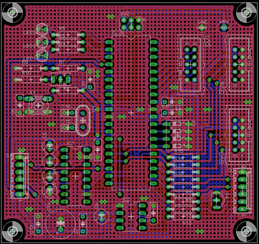
Front Panel IO Schematic and PCB Layout
Right click and then "save as" to see these images at higher resolution. The board Eagle files are available for download below.
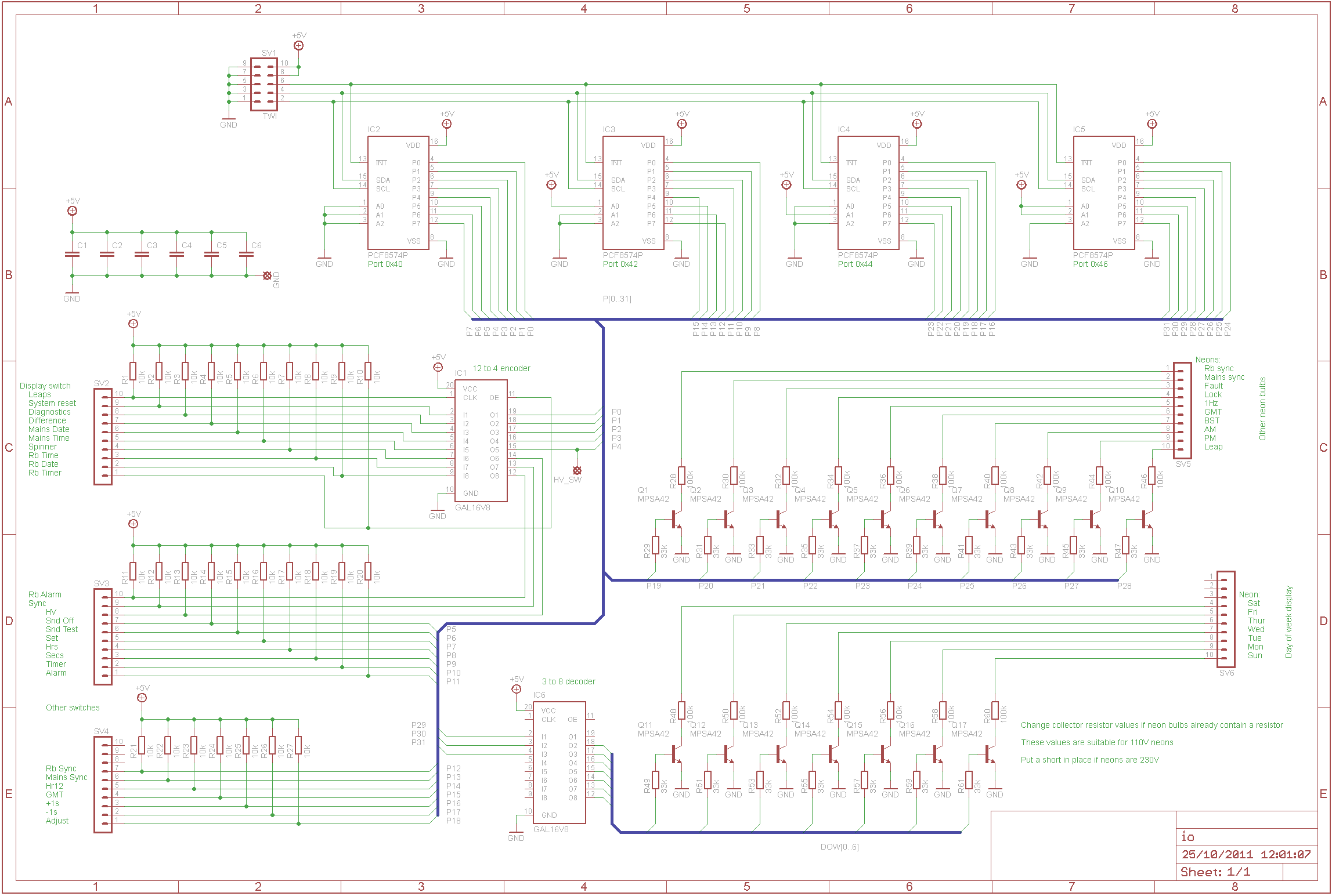
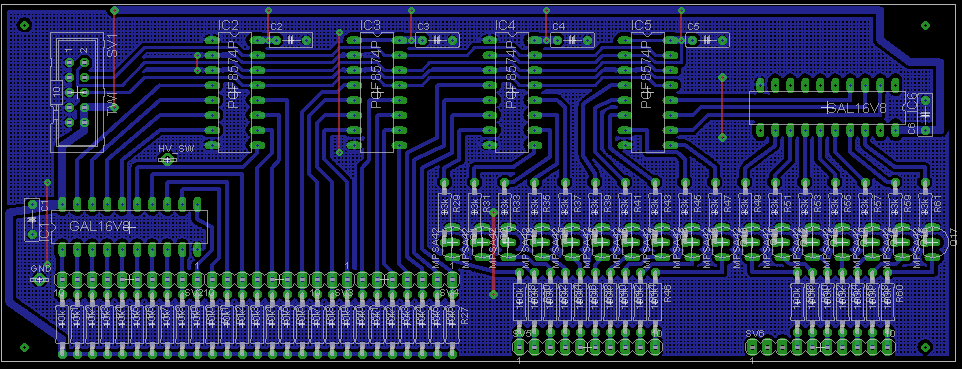
The final board has high voltage transistors to drive 17 neons and can read 27 switch inputs.
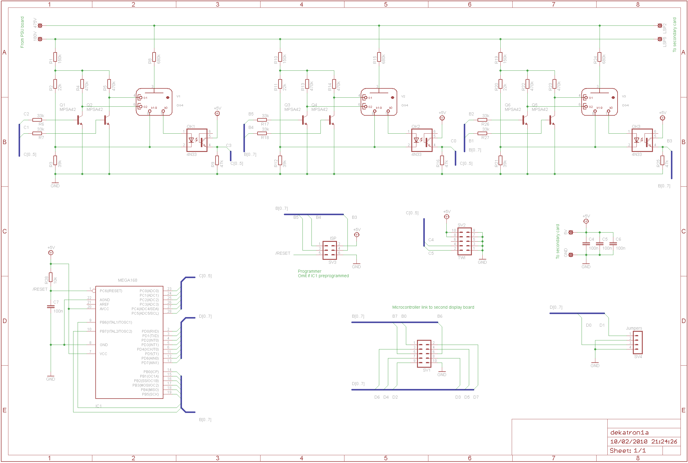
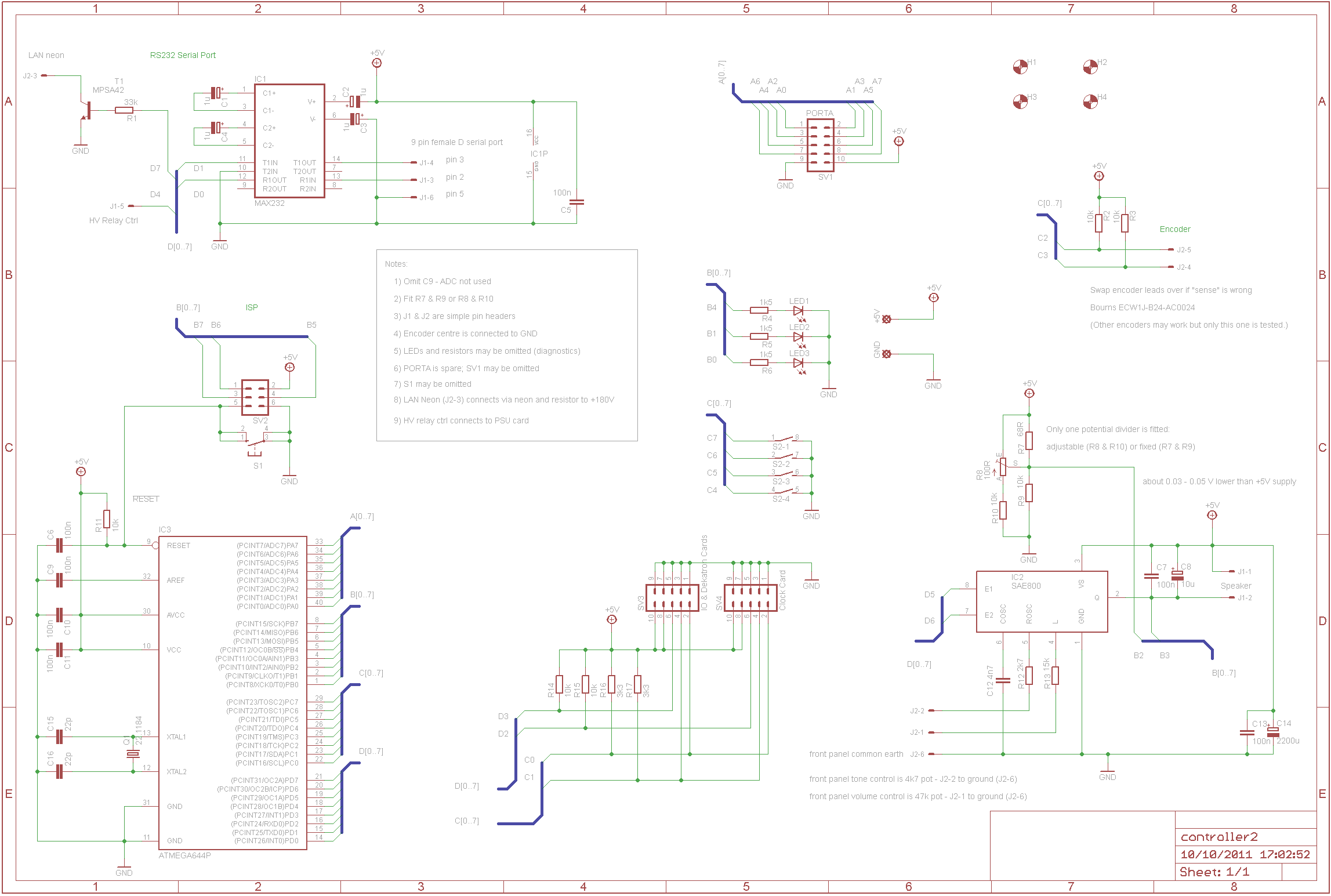
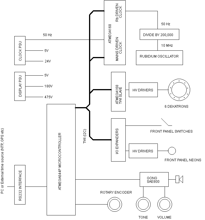
Main Microcontroller

The last board to describe is the main micocontroller board. The board has the following facilities:
- RS232 interface to be able to synchronise the rubidum clock with an external time source such as a GPS unit or NTP Client, to link to a PC for diagnositics and other setup and to provide a serial link to a data network (for example using RS485)
- SAE800 gong chip to generate tones for alarms, hour chimes etc
- A TWI interface for use within the clock to communicate with the front panel controls, the dekatrons and the clock TWI slaves (all described above) (brought out on two headers)
- Interrupt inputs from the rubidium oscillator timed clock to give an accurate 1 interrupt per second and an interrupt from the front panel I/O expanders that will interrupt to signal that front panel switch has been moved
- 4 way DIL switch to options that I would not anticipate changing very often (in that you need to open the case)
- 3 LEDs for simple diagnostics and testing purposed
- A rotary encoder to be able to adjust clock alarm and timer settings
- A hardware reset button
- A whole spare port (Port A) brought out to a box header
- Finally, a programmer socket (in-situ programmer or ISP)
I selected an ATMEGA644P-20 (to be slightly overclocked at 22.1184 MHz) as it contains a genererous amount of flash, SRAM, EEPROM (not that I envisaged using much EEPROM use in this project) and sufficient I/O pins, UARTs etc for all of the facilities listed above. Again, here is the schematic and PCB layout (another double sided board) to view and the designs are in the Eagle download file.
Main Microcontroller Schematic and PCB
Right click and then "save as" to see these images at higher resolution. The board Eagle files are available for download below.
SAE800 Gong Chip
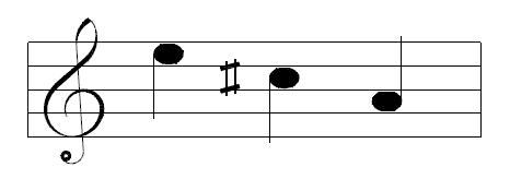
The gong chip is probably worth a special mention as it is a simple way to get single, dual or triple gong tones. In the triple tone mode the notes, for example can be arranged as the minor and major third: e2 - c# - a, corresponding to 660Hz, 550Hz and 440 Hz.
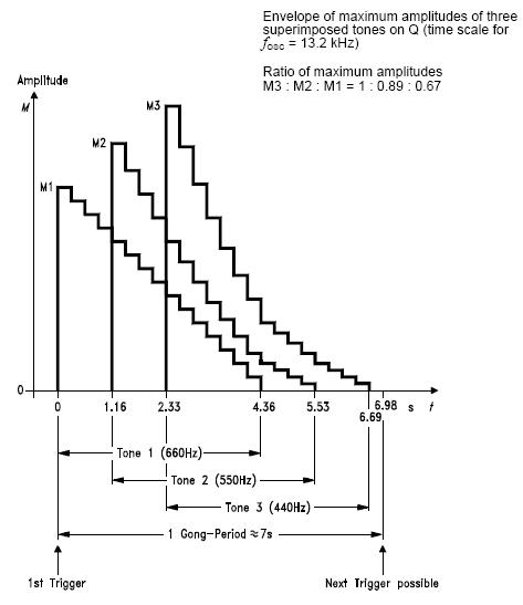
The gong chip allows the tone fundamental frequency and volume to be adjusted by setting two resistor values, so I decided to bring these out as variable resistors on the front panel (well why not?). Here is a (crude) recordings with a microphone of the gong chip in action:
Three tone test MP3:
The gong chip is simple to use and triggering it is easy in the software. The downside is that it is a bit municipal rather than musical.
Design Summary
The main elements of the clock evolved to be:
- A power supply for the rubidium oscillator and clock chips (24V and 5V). This power supply has 24V batteries to keep the rubidium clock alive during power outages
- A switchable power supply for the display elements, 475V for the dekatron anodes, 180V for the front panel neon bulbs and dekatron guide electrodes
- 5V supply for the controller and display electronics
- RS232 interface for sychronisation with an external time source or PC
- A rotary encoder for setting other values
- SAE800 gong chip for chimes and alarms
- A TWI bus
- A rubiduim oscillator and divider down to 50 Hz
- A clock run from the rubidium oscillator - using an ATMEGA168 as aTWI slave
- A clock run from mains frequency (either 50Hz or 60Hz) using the same ATMEGA168
- 6 dekatrons controlled by a second ATMEGA168 again as a TWI slave
- A front panel of switches and neons driven by TWI I/O expanders
All schematics and PCBs
The boards are a mixture of single and doubled sided. The single sided boards often have a few wire links required. The double sided boards have many wire links or require leaded components (diodes, resistors, etc) to be solder both sides. Care if needed to make all the required solder joints! In particular, the divider card has a few links that bridge over signal leads on the top surface.
Software
The complete source code, compiled hex files and notes on the required fuse settings for the three AVRs used will be eventually be available to download. I am rewriting most of the code during 2010/11… so it will be a while yet. That said, this download includes all of the code for the dekatron and divider card slaves, and the test code descrbed in the annexes below. Development has stopped - these updates ain't going to happen. But See Atomic Clock II.
The source and jedec files for the two GAL16V8 chips on the front panel I/O card can be downloaded below. I use the free WinCupl compiler from Atmel.
Case selection, front panel and assembly
Originally I used a home made front panel, the design is now in an annex towards the end of this page. To improve the appearance of the clock I had a front panel professionally made - laser cut, engraved, the works. Not a cheap option as it came to just over €150 but the clock appearance was markedly improved.
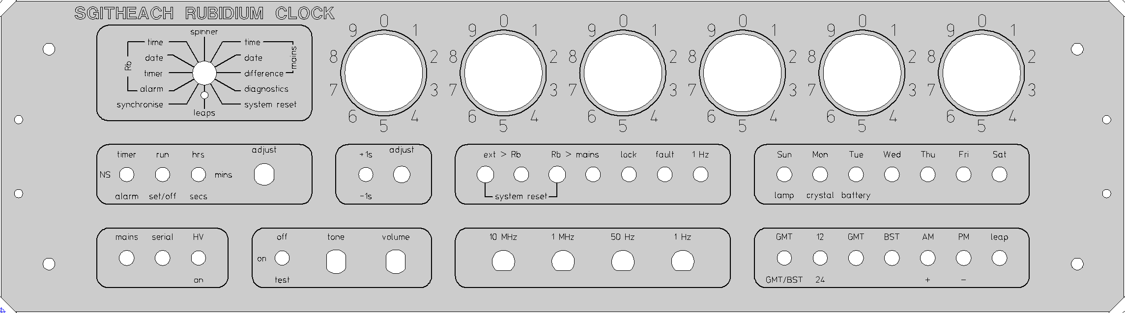
The lines on this image are very thin so you will need to save or view it to see the detail.
The panel was manufactured by Schaeffer AG. You download the design software from their website and then the ordering is entirely online. I have found their service painless and faultless. My front panel design file can be downloaded from the dropbox. Should you want to use this layout, you must check, especially, the drill hole sizes, the use of D (or double D) holes for components with flats on the threads and the locking hole on the mode switch (size and position), to ensure everything fits your components. Change the labelling, the title and so on, according to your taste. Additionally, this panel was designed for GC10B dekatrons and you should check the dekatron hole sizes if you are using OG4 dekatrons.
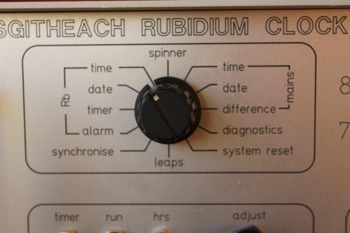
| Purpose | Device | Function |
| mode | 12 position rotary switch |
|
| mains | red neon | mains is plugged in and switched on |
| serial | green neon | flash during activity on the serial port |
| HV | submin toggle |
Switch on high voltage PSU; when off the dekatrons and all neons except the mains neon will not glow; the clock otherwise operates as normal |
| timer-off-alarm |
3 position submin toggle |
|
| run-set | submin toggle |
timer or alarm is selected above
|
| hrs-mins-secs |
3 position submin toggle |
When "set" is selected the dekatrons will show the timer period remaining or the alarm time the rotatry encode can be used to change the value
|
| adjust | rotary encoder |
This control has several uses depending on the setting of the mode switch or if an alarm or timer is being adjusted
|
| off-on-test |
3 position submin toggle on-off-(on) type |
|
| tone | potentiometer | change the frequency and speed of the chimes |
| volume | potentiometer | change the loudness of the chimes |
| +1s -1s |
3 position submin toggle (on)-off-(on) type |
Make a precise 1 second change to the Rb clock; (e.g. on a leap second change) the switch is held in the + or - position and adjust is pressed |
| adjust-spinner |
momentary action push button |
Use depends on mode switch
|
|
ext > Rb system reset |
momentary action push button |
Use depends on mode switch
|
| ext > Rb | orange neon | neon will go out when synchronisation is complete |
|
Rb>mains system reset |
momentary action push button |
Use depends on mode switch
|
| Rb>mains | orange neon | neon will go out when synchronisation is complete |
| locked | green neon | the Rb oscillator reports that it is locked |
| fault | red neon | the Rb oscillator reports it has a fault |
| 1 Hz | green neon | will flash once per second based on the Rb clock second count |
| signal outputs | BNC |
These are TTL level squarewave signals from from the Rb oscillator and divider chain |
| Day of week | 7 orange neons |
Use depends on mode switch
|
| GMT-GMT/BST | submin toggle |
|
| 12-24 | submin toggle |
|
| GMT | red neon | date & time shown is GMT |
| BST | green neon | date & time shown is BST |
| AM + | red neon |
Use depends on mode switch
|
| PM - | green neon |
Use depends on mode switch
|
| leap | red neon | if a date is shown then it is a leap year |
A word about fault conditions. The fault neon (and the fault LED on the divider card) will light if the Rb oscillator/divider reports any of the following:
- The oscillator is not locked
- The crystal voltage is not in the range 5.5-12.6 volts
- The lamp voltage is not in the range 3.0-12.0 volts
- The battery voltage is not in the range 18.0-27.6 volts
Photo Gallery
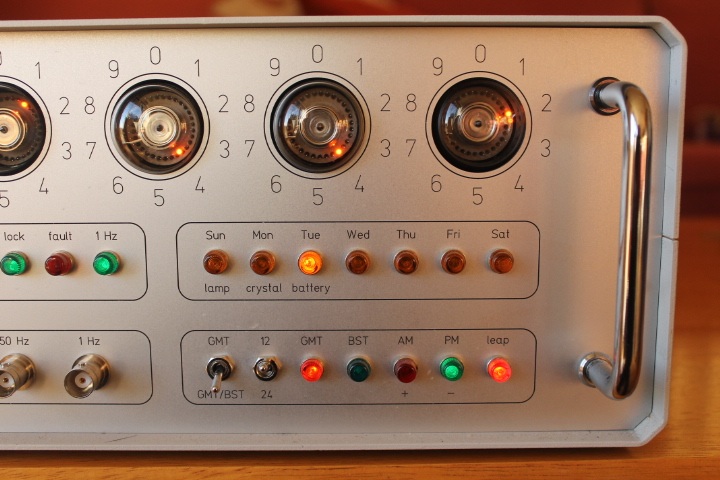
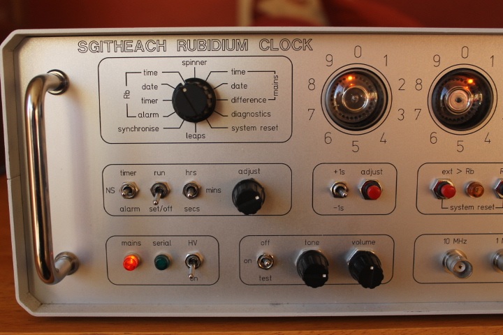
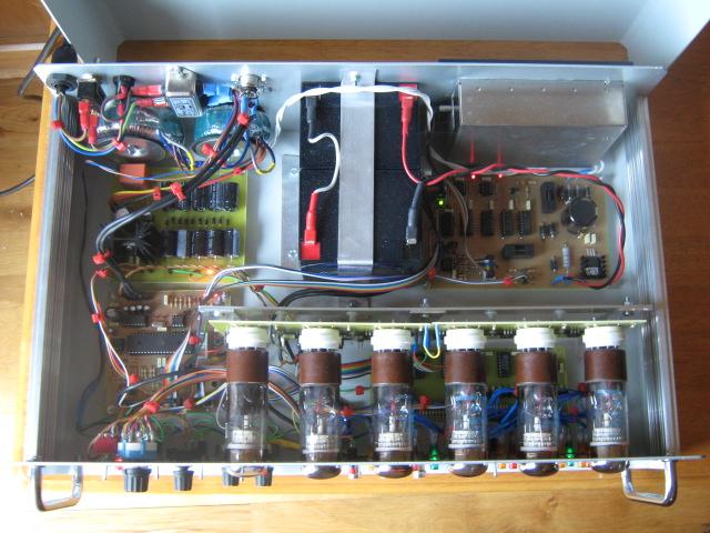
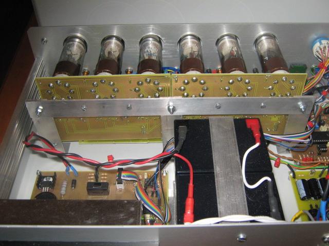
So am I please or what?!?
Annexes
Construction notes
The notes and schematics above are far from complete and so I will try to fill in some of the gaps. The wiring between the front panel and the PCBs has to be made precisely or else things won't work as expected of course. You could adopt different wiring but you will also need to amend the code in the main controller and the IO test software. The types of the various front panel controls needs to be listed and so on. So without much more ado.
Front panel controls
| Use | Description |
IO Card Connection (or as described) |
| Mode switch | 1 pole 12 position rotary |
Leap seconds SV2-10 System Reset SV2-9 Diagnostics SV2-8 Difference SV2-7 Mains Date SV2-6 Mains Time SV2-5 Spinner SV2-4 Rb Time SV2-3 Rb Date SV2-2 Rb Timer SV2-1 Rb Alarm SV3-10 Synchronise SV3-9 |
| knob for above | ||
| alarm/off/timer switch | submin toggle: on-off-on |
Timer SV3-2 Alarm SV3-1 |
| run/set switch | submin toggle: on-off | SV3-5 |
| hrs-mins-secs switch | submin toggle: on-off-on |
Hrs SV3-4 Secs SV3-3 |
| rotary encoder | Alps ECW1J-B24-AC0024 |
wired to main controller card J2-4 & J2-5 |
| knob for above | ||
| mains on neon | red | wired to back panel after LC filter |
| serial activity neon | green |
wired to main controller card J2-3 |
| +1s/-1s adjust | submin push button non-latching |
+1s SV4-3 -1s SV4-2 |
| chime switch | submin toggle: on-off-(on) |
off SV3-7 test SV3-6 |
| tone control | 4k7 pot |
wired to main controller card J2-2 |
| knob for above | ||
| volume control | 47k pot |
wired to main controller card J2-1 |
| knob for above | ||
| Rb clock sync |
submin push button non-latching |
SV4-7 |
| Rb sync done neon | orange | SV5-1 |
| mains clock sync |
submin push button non-latching |
SV4-6 |
| mains sync done neon | orange | SV5-2 |
| Rb locked neon | green | SV5-4 |
| Rb fault neon | red | SV5-3 |
| Rb 1Hz neon | green | SV5-5 |
| signals out (4 off) | BNC | wired to divider card |
|
day of week neons (7 off) |
orange |
Sunday SV6-10 Monday SV6-9 Tueday SV6-8 Wednesday SV6-7 Thurday SV6-6 Friday SV6-5 Saturday SV6-4 |
| GMT/BST switch | submin toggle: on-off | SV4-4 |
| 12/24 hr switch | submin toggle: on-off | SV4-5 |
| GMT neon | red | SV5-6 |
| BST neon | green | SV5-7 |
| AM neon | red | SV5-8 |
| PM neon | green | SV5-9 |
| leap year neon | red | SV5-10 |
Obviously the items might change depending on your personal taste. The colour of neons is yours entirely; I have just listed the colours I used. Some neons have built in resistors - you may need to change the series resistors on the IO board accordingly. Other rotary encoders should work, but the item listed is the one I have used and tested.
Back panel
On the back panel I mounted a mains cable gland, a DPDT mains on/off switch, a fuse holder, a small LC mains filter (the one I used is marked FA-3Z), the two mains transformers, 9 pin female D socket (serial port) 3 pin DIN socket (5V power out) and a heatsink behind the Rb oscillator module. If you look at the photo gallery you will see how these items are used. Mains is fed from the LC filter output to a neon on the front panel. My neons were 110V so a put an additional 120k resistor in series.
Testing
To facilitate the testing and set up of the 6 PCBs that make up the clock a series of test programs were written. In the description below [X] means a key to press, X in this case. All of the test programs are case insensitive so [X] and [x] provoke the same effect; [0]..[2] indicates a range, [0], [1] or [2] in this case.
PSU
Obviously no software involved! Just make sure that the correct output voltages are present. To test the HV outputs the relay switch transistor need to have 5V applied to the input pin. The high voltages measured should be on the high side when off-load and the voltages rechecked when on-load. The 5V regulator should be checked for overheating when on-load.
Main Controller - tests other than TWI
The following tests are made:
- LEDs
- output to HV switch
- output to serial neon
- chime generation, timing and queuing
- switch inputs
- RS232 serial port
- rotary encoder
- PortA outputs
To test the main board make the following temporary connections:
- RS232 input, output and ground to a 9 pin female D type and connect to a PC serial port (57600,N,1)
- connect a rotary encoder
- connect a speaker, the volume pot and the tone pot
- connect a LED and 1k resistor from HV relay output to ground
- connect a LED and 1k resistor from LAN neon output to + 5V
- power the board with 5V
Program mega with code and set fuses (all test programs use the same fuses) Run software in AVR - press [?] to get listing of commands (this will demonstrate that the mega is running and the serial port is ok.
The unused PORTA outputs are toggle incrementally at 5 Hz - pins can be inspected for square wave. Expect 5Hz on pin 0 to 5/256 Hz (one cycle in about 25 seconds) on pin 7.
The rotary encoder should report '+' when moved clockwise and '-' when moved anticlockwise. Swap its leads if the reverse happens. I suggest that you note the wiring connections so correct sense connections are made the when board is wired to the encoder mounted on the front panel.
You may also experiment with C12, R12, R13, tone control pot and volume control pot to get tone/volume range which is pleasing for you. Values may be dependant on the speaker used (especially the volume control settings and how the speaker is finally mounted in the case). Note that the volume cannot be reduce to zero.
Anything non-functional should be repaired before continuing.
A command is just a single keystroke which is acted on immediately. The full list of commands is:
- [0]..[9] [-] [=] queue 1..12 single chimes
- [A] play single chime
- [B] play double chime
- [C] play triple chime
- [D] queue single chime
- [E] queue double chime
- [F] queue triple chime
- [+] toggle chime silence
- [L] flash LEDs in sequence
- [H] toggle HV switch output
- [N] toggle serial neon output
- [S] report switch positions
- [Z] calibrate chimes
So the 12 keys [0]..[9] [-] and [=] simulate the hourly chimes. ABC play chimes immediately - pressing the key too early will be ignored. DEF play chimes but they are queued so pressing a key will place it in a queue which is slowly emptied. The queue has space for 20 chimes and an error message will be produced if you try to overfill the queue (the hourly chimes are queued as well so press [=] twice quickly to provoke the error message). The [+] key will silence the chime. When the chimes are playing you will see the LEDs light as the chime is sounded and the queue emptied.
[L] will flash each LED is sequence (overriding the use by the chimes).
[H] will toggle the HV switch output as indicated by the LED.
[N] will toggle the serial neon output as indicated by the LED.
[S] will report the position of the 4 on board rocker switches.
[Z] will cause the triple chime to sound. This is timed by the controller so the time can be used to play the chime sequence. Whenever the tone control is changed this calibration step must be made or the chime sequence may not play properly. Chimes may be omitted or the chime sequence may be overly long. (The chime calibration will be performed when the chime "test" switch is pressed on the front panel.)
Chime testing is where the three LEDs come in useful. The first LED is connected to the mega analogue compare output so it lights when the chime is playing, but pulses as the chime decays. The controller software smooths the pulses and so the second LED lights without pulsing when a chime is playing. Finally, third LED lights when the chime queue is not empty. Inspecting the outputs from the mega for LED1 and 2 on a dual channel 'scope should illustrate what is happening (step not essential, just for the curious).
Divider card
The two clocks on the divider card operate independantly of the main controller. When the AC supply is connected the mains clock 1Hz LED will flash.
With the Rb oscillator connected as well the Rb clock 1Hz LED will flash and after a few minutes the locked LED should come on. If the fauilt LED remains lit or if the locked LED doesn't light then it should be investigated.
If you can test the outputs you should find 10MHz, 1MHz, 50Hz and 1Hz TTL level square waves. To check the frequencies you need test equipment that is better than the Rb clock. My cheap frequency counter reports 10,000,100 Hz - which is suprisingly good, the counter that is.
Further testing can be carried out using the main controller card. The test software is programmed into the mega644p and the serial connection made to a PC (57600,8,n,1) and a 10 way ribbon cable used to connect the two cards together. The ribbon cable must be plugged into the 10 way header SV4 (in the corner of the board and parallel to the Port A 10 way header. Supply 5V to the controller card.
The command are typed in and return pressed to execute the command. There are no editing functions - this is just a crude text input. The commands are:
- [?] help message
- [B] report Rb date time
- [D] dd-mm-yyyy hh:mm:ss set Rb clock date and time
- [M] report mains date time
- [R] reset clock card (takes upto 2 seconds)
- [S] sync mains clock to Rb clock
- [T] battery,lamp,xtal - ADC trim values (base 1000)
- [X] Rb status
- [Y] misc information
[B] reports the date and time accordinging to the Rb based clock.
[D] allows you to set the date and time of the Rb based clock. The millisecond counter is set to zero. The format must be exactly that shown above.
[M] reports the date and time accordinging to the mains based clock.
[R] forces the card to reset. This may take upto 2 seconds. The current date and time is lost from both clocks.
[S] will sync (i.e. copy) the date and time from the Rb clock to the mains clock.
[T] allows the conversion of various voltages on the card to be trimmed. I used only 5% tolerance resistors and allow for the variation in values to be adjusted here. The procedure is to measure the actual voltages presented to the potential dividers R3/R5 for the battery voltage, R11/R18 for the lamp voltage and R12/R19 for the crystal voltage. The X command will report these voltages as measured by the ADC from these potential divider taps. You can now enter the T command (e.g. T 1003,1004,997) to make small adjustments to trim the actual measurement to the ADC measured values. The adjustment values should be very close to 1000, otherwise a fault must be suspected. The entered values are now stored in eeprom on the divider card and should not need changing again unless the controller is reprogrammed/replaced etc. This step is not essential for correct operation of the clock.
The default values of 1000,1000,1000 can be reset by placing a jumper across the "force defaults values" pins 5 and 6 on SV2 and reseting the controller.
[X] reports the Rb status information namely:
- the locked status: 1 = locked, 0 = unlocked
- the error status: 1 = error, 0 = no error
- the battery voltage
- the lamp voltage
- the crystal voltage
- the TWI data frame CRC7 value (ignore)
[Y] reports a bunch of miscellaneous information:
- 50Hz/60Hz mode jumper: 1 = fitted = 60Hz, 0 = open = 50Hz
- "force default values" jumper: 1 = force = fitted, 0 = open
- the battery, lamp and crystal adjustment values
- the divider card software version number: major.minor.build
- the TWI data frame CRC7 value (ignore)
I would recommend entering a data and time into the Rb clock, sync the Rb and mains clocks and then leave running for hours or preferably a few days. The date and time should not drift at all, or at least that you'll notice.
IO Card Testing
The purpose of these tests is to check the wiring between the front panel and the IO card, and the TWI link between the IO card and the main controller. So this software is used after the IO card is installed and the front panel wired.
The volume control, tone control, rotary encoder, mains neon, serial neon, dekatrons and the frequency outputs are not tested here because none route signals through the IO card.
Program mega with code and set fuses (all test programs use the same fuses) Run software in AVR - press [?] to get listing of commands (this will demonstrate that the mega is running and the serial port is ok.
The IO card and controller are linked using a 10 way ribbon cable. The cable must be plugged into header SV3 on the controller card (next to the 4 switches).
A command is just a single keystroke which is acted on immediately. The full list of commands is:
- [0] Set DOW to Sunday
- [1] Set DOW to Monday
- [2] Set DOW to Tuesday
- [3] Set DOW to Wednesday
- [4] Set DOW to Thursday
- [5] Set DOW to Friday
- [6] Set DOW to Saturday
- [A] AM on, PM off
- [B] BST on, GMT off
- [E] leap toggle
- [F] fault toggle
- [G] GMT on, BST off
- [L] lock toggle
- [M] mains sync toggle
- [P] PM on, AM off
- [R] Rb sync toggle
- [Z] chaos toggle
- [-] all neons off
- [space] or [return] Switches & buttons report
[0]..[6] will light a day or week neon
[A] and [P] will light the AM/PM neons
[B] and [G] will light the BST/GMT neons
[E] will toggle the leap neon on/off
[F] will toggle the fault neon on/off
[L] will toggle the Rb locked neon on/off
[M] and [R] will toggle the mains and Rb sync neons on/off
[-] will turn all neons off
[Z] is a bit of fun, nothing more
[space] or [return] keys will report the status of the front panel switches. Some switches don't lock in position so must be held in position while [space] or [return] is pressed to check the result.
The 1 Hz neon will flash once per second.
Whenever a switch position is changed LED1 will flash. This shows that the mega has received an interrupt from the IO card. The switch positions are only read after this interrupt has been received. LED2 flashes once per second and LED3 flashes on any keystroke.
Dekatron Card Testing
The dekatron card has a simple self test mode - put a jumper on pins 1 & 2 of SV4 and the dekatrons should cycle through the range of spinners and repeat continuously.
Further testing can be carried out using the main controller card. The test software is programmed into the mega644p and the serial connection made to a PC (57600,8,n,1) and a 10 way ribbon cable used to connect the two cards together. The ribbon cable can be plugged into either 10 way header SV3 or SV4. Supply 5V to the controller card. Optionally, pin J1-5 on the main controller card can be connected to the HV relay switch input on the power supply card.
The command are typed in and return pressed to execute the command. There are no editing functions - this is just a crude text input. The commands are:
- [?] help message
- [B] 0 | 1 backward movement flag: 1=permitted; 0=not permitted
- [D] a b c d e f position dekatron 1 (RH) to dot "a" (0-29); dekatron 2 to dot "b" etc
- [H] 0|1 High Voltage status: 1=on; 0=off
- [M] x set display mode "x" (1-21) see below
- [N] a b c d e f position dekatron 1 to number "a" (0-9); dekatron 2 to number "b" etc
- [P] x y set dekatron "x" (1-6) to dot "y" (0-29)
- [R] reset the dekatron card (takes upto 2 seconds)
- [S] n wait "n" mS during spinner steps (0-255) (default 100)
- [V] n wait "n" mS bewtween dot position moves (0-255) (default 10)
- [W] n spinner wave dot lag (0-29)
- [Y] report miscellaneous infomation
- [Z] zero all dekatrons
[B] allows backwards (anticlockwise) dot movement, otherwise the dot is only permited forwards (clockwise) movement. The default is to allow backwards (bidirectional) movement. Turning off backwards movement can cause some strange effects (try it and see).
[D] allows you to set the dot position of each dekatron simultaneously. The right had dekatron is number 1; the lefthand dekatron is number 6. This command sets the dot position as against aligning the dot to a numbered location. So the dot can stop on a guide electrode. Dots are numbered 0-29 and the numbered locations are 0-9 corresponding to dot locations 0, 3, 6, 9 etc. See also the N command below.
[H] HV status 1=on; 0=off; this command can simulate the absence of the HV supply without actually switching it on and off; if the pin J1-5 on the main controller card is connected to the HV relay switch input on the power supply card then the HV can be switched in anger.
[N] allows the number position of each dekatron to be set simultaneously. See the [D] command above for an explaination.
[M] set the display mode; modes available are as follows:
- Positioning - effectively the same as mode 2. for the purpose of this test command
- Stop - all dekatron motion stops
- Zero - all dekatrons are zeroed and stopped
- All dekatrons spin synchronised clockwise
- As 4. but anticlockwise
- All dekatrons spin clockwise but each dekatron has a number of dots lag behind the dekatron on its left hand - the effect is a wave; see [W] command
- As 6. but anticlockwise
- The rightmost 3 dekatrons spin clockwise and the 3 leftmost dekatrons spin anticlockwise
- As 8. except the spin directions are reversed
- As 8. but as a wave
- As 9. but as a wave
- The dekatrons dots are randomly positioned (chaotic)
- A short arc pendulum
- A medium arc pendulum
- A long arc pendulum
- Rotate once clockwise stopping back at the starting position
- As 16. but anticlockwise
- The dekatrons "point" to the 3 o'clock position and stopped not returned to starting positions
- As 18. but 6 o'clock
- As 18. but 9 o'clock
- As 18. but 12 o'clock
See also [S] and [V] command for control of speeds.
[N] See the [D] command above except that the parameters are ranged 0 - 9 and the dekatrons are positioned by number (0-9) rather than dot.
[P] Positions a single dekatron (1-6) to a given dot position (0-29).
[R] Reset the controller. May take upto 2 seconds. The spinner step timing (see [S] and dot move timing (see [V]) are reset to there default values.
[S] mS wait between spinner steps from the range 0mS (as fast as possible) to 255mS. The default value is 100mS so a single orbit of 30 steps takes 3 seconds. At 250mS (¼S) an orbit takes 7.5S; less than about 5mS the dot is just a blur.
[V] mS between dot movements other than in spinner or other prefined movement patterns. This is used when the glow position is being moved, for example, as the time or date is changing. It allows the intermediate dots to be seen to glow briefly. Use the command P 1 15 and P 1 0 and vary the timing to see how the V command slows the dot movement speed down. The default value is 10 mS which allows the dots to be visible, but as a blur (the worst case is a movement of 15 dots which will take 150mS). Too high a value will cause problems as the dot may not have completed its traverse to a new value before the next movement command is sent.
[W] wave mode dot lag factor - I find about 6 pleasing. But try the range 1 - 29… The value 0 is trivial in that the dekatrons are just synchronised together. Values above 29 may cause weird or random effects.
[Y] reports a bunch of miscellaneous information:
- demo mode jumper: 1 = fitted = demo, 0 = open = normal operation
- spare jumper: 1 = fitted, 0 = open
- the dekatron card software version number: major.minor.build
- the TWI data frame CRC7 value (ignore)
[Z] Set all the dekatrons to number (and dot) position 0 and stop movement.
Operational Menu
A number of options are not set using the front panel controls. My original idea was little changed options would be be set by the 4 switches on the main PCB. However, I quickly realised that something more complex would be required.
Entering ? or HELP will produce a listing of the available commands. Values can be reported and, in many cases, changed. Changed values are saved to EEPROM and are reloaded when the clock starts.
Construction afterword
I hope I have fully and accurately documented the switch and neon connections! My apologies for any mistakes!
Original Front Panel
For the first version of the front panel I drew the front panel design in Eagle (using the Eagle schematic editor). The image was printed onto two A4 sheets of a sticky backed "quick-laser label system" film with a silver finish stocked by Rapid Electronics in the UK. I had to use two sheets with a butt joint (between the leftmost and second dekatrons) but the overall front panel I don't think was spoilt.
The Eagle download below contains this drawing together with a second older version that contains construction lines to assist the layout of the front panel which, obviously I deleted for the final printed version.
Downloads
You should look in the "/Dekatron Projects/Atomic Rubidium Dekatron Clock 1" folder.